Silicon-on-insulator lateral n-type insulated gate bipolar transistor

A bipolar transistor, silicon-on-insulator technology, applied in semiconductor devices, electrical components, circuits, etc., can solve the problems of increasing channel length, changing to P-type, and reducing gate turn-off performance, so as to reduce conduction The effect of increasing the resistance, increasing the lateral withstand voltage, and increasing the conduction current

Active Publication Date: 2020-07-03
SUZHOU POWERON IC DESIGN
View PDF9 Cites 0 Cited by
  • Summary
  • Abstract
  • Description
  • Claims
  • Application Information

AI Technical Summary

Problems solved by technology

However, there is still a parasitic PNPN thyristor structure in SOI-LIGBT. If the sum of the current gains of the NPN transistor and the PNP transistor in the equivalent circuit of the parasitic NPNP thyristor structure is equal to or greater than 1, the PNPN thyristor is When it is turned on, the turn-off performance of the gate is reduced, which is called latch-up, which will lead to device damage in severe cases
Therefore, in the related art, in order to reduce the possibility of latch-up, some people propose to add P-type doped deep well region 5 in SOI-LIGBT, but due to the high concentration of P-type doped deep well region 5, the lateral diffusion The ability is also very strong, so in the process manufacturing engineering, the lateral diffusion of the P-type doped deep well region 5 will make the length of the effective channel longer, and it is possible to make the N-type at the right end of the low-concentration N-type doped semiconductor region 6 The impurity concentration is very low and even becomes P-type. In order to solve this problem, someone proposes to increase the length of the gate so that the gate covers the right part of the N-type doped semiconductor region 6. Although it can ensure that the SOI-LIGBT is normally turned on, this This method increases the length of the channel and reduces the conduction current of SOI-LIGBT

Method used


Image

  • Silicon-on-insulator lateral n-type insulated gate bipolar transistor
  • Silicon-on-insulator lateral n-type insulated gate bipolar transistor

Examples


Embodiment Construction

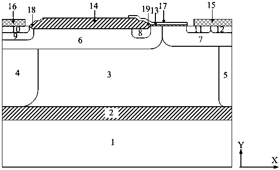
[0014] refer to figure 1 , a silicon-on-insulator lateral N-type insulated gate bipolar transistor, comprising: a P-type doped semiconductor substrate 1, a buried oxide layer 2 is arranged on the P-type doped semiconductor substrate 1, and a buried oxide layer 2 is arranged on the buried A P-type doped epitaxial layer 3 is arranged on the oxygen layer 2, an N-type doped deep well region 4 is arranged on the left side of the P-type doped epitaxial layer 3, and an N-type doped deep well region 4 is arranged on the right side of the P-type doped epitaxial layer 3. A P-type doped deep well region 5 is provided on the side, an N-type doped drift region 6 is arranged above the N-type doped deep well region 4 and part of the P-type doped epitaxial layer 3, and an N-type doped drift region 6 is arranged on the P-type doped deep well region 4 and part of the P-type doped epitaxial layer 3. A P-type doped semiconductor region 7 is arranged above the P-type doped deep well region 5 and p...


PUM


Abstract

The invention discloses a silicon-on-insulator lateral N-type insulated gate bipolar transistor, comprising: a P-type doped semiconductor substrate, a buried oxide layer is arranged on the P-type doped semiconductor substrate, and an oxide layer is arranged on the oxide layer. The N-type drift region is provided with a higher concentration N-type doped semiconductor region in the N-type drift region. This higher concentration N-type doped semiconductor region is located under the second bird's beak region at the right end of the field oxide layer and surrounds the entire The concentration of the bird's beak region is higher than that of the N-type drift region. At the same time, the anode contact region of the device is formed by alternating arrangement of P-type doped regions and N-type doped regions in the width direction of the device. Moreover, the field oxide layer of the silicon-on-insulator lateral insulated gate bipolar transistor belongs to a two-layer stepped field oxide layer, and the field plate formed by extending the gate to the top of the field oxide layer is also a second-order field plate, which can effectively improve the performance of the device. Horizontal withstand voltage level.

Description

technical field [0001] The invention belongs to the technical field of integrated circuits, and relates to a lateral high-voltage power device, more specifically, a silicon-on-insulator lateral N-type insulated gate bipolar transistor with fast switching speed and large conduction current. Background technique [0002] An insulated gate bipolar transistor (IGBT) is a device that has the advantages of an insulated gate structure of a metal oxide semiconductor (MOS) transistor and the advantages of high current density of a bipolar transistor. It is a device that can be used to effectively reduce the traditional Power MOSFET (Metal Oxide Semiconductor Field Effect Transistor) is a power semiconductor device with conduction losses. [0003] In order to be able to integrate with other semiconductor devices, Lateral Insulated Gate Bipolar Transistor (LIGBT for short) has received extensive attention and rapid development. Similarly, this device has high input impedance, high with...

Claims


Application Information

Patent Timeline
Patent Type & Authority Patents(China)
IPC IPC(8): H01L29/739H01L29/06H01L29/36
Inventor 李海松王钦刘侠杨东林陈文高祝靖刘斯扬易扬波
Owner SUZHOU POWERON IC DESIGN
Why Eureka
Try Eureka