

Manufacturing method of semiconductor device and semiconductor device
A manufacturing method and semiconductor technology, applied in the field of semiconductor device and semiconductor device manufacturing, can solve the problems of enlarging component isolation area, performance degradation of semiconductor device, high density of difficult pixels, etc., and achieve the effect of improving performance and preventing characteristic deviation
- Summary
- Abstract
- Description
- Claims
- Application Information
AI Technical Summary
Problems solved by technology
Method used
Image

Examples
no. 1 Embodiment approach
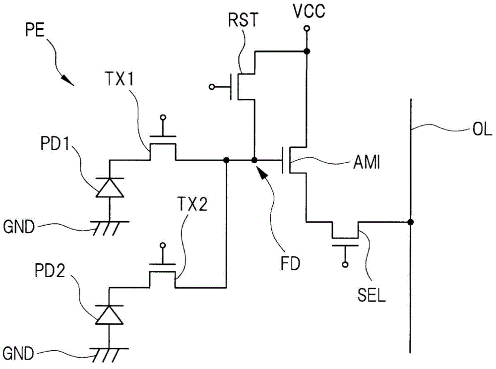
[0050] pass below Figure 1 to Figure 6 The semiconductor device in this embodiment mode will be described. The semiconductor device in this embodiment mode is related to a solid-state image sensor, particularly a solid-state image sensor having a plurality of photodiodes in one pixel.
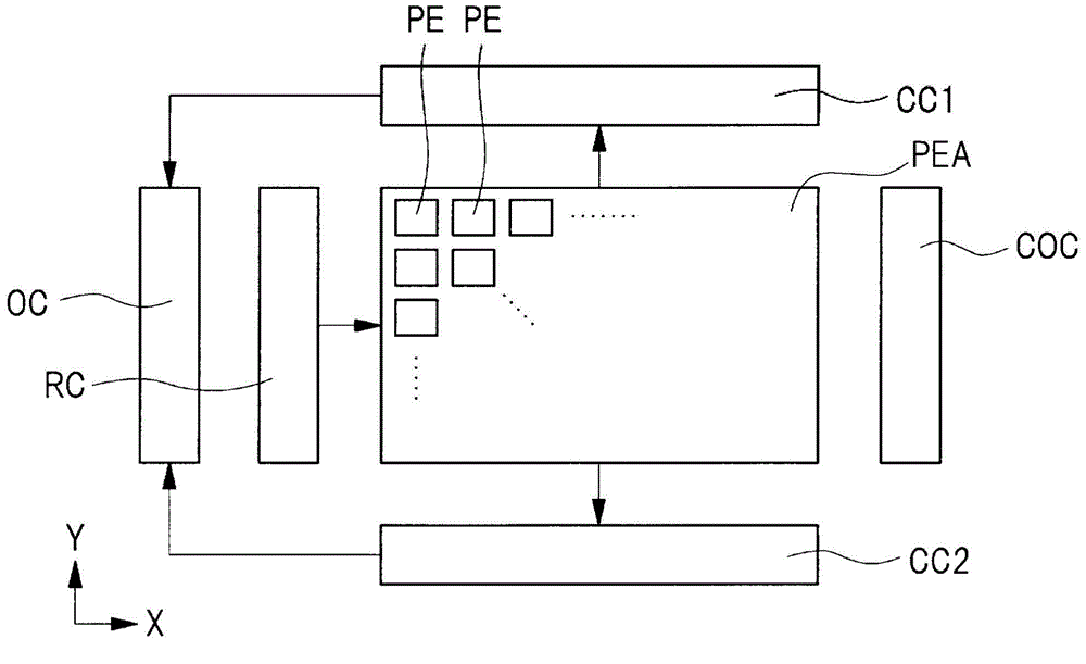
[0051] figure 1 Shown is a schematic diagram of the structure of the solid-state image sensor related to the first embodiment of the present invention. The semiconductor device in this embodiment, that is, the solid-state image sensor is a CMOS (Complementary Metal Oxide Semiconductor, Complementary Metal Oxide Semiconductor) imaging sensor. Such as figure 1 As shown, the solid-state image sensor has a pixel array unit PEA, readout circuits CC1, CC2, an output circuit OC, a row selection circuit RC, and a control circuit COC.
[0052] In the pixel array unit PEA, a plurality of pixels PE are arranged in rows and columns. figure 1 The indicated X-axis direction is a direction along the mai...
no. 2 Embodiment approach
[0158] In this embodiment, the case where the distance between the photodiodes arrayed in the pixel can be increased by shifting the formation positions of the photodiodes in the pixels which coincide with the boundary line of the divided exposure is shifted.
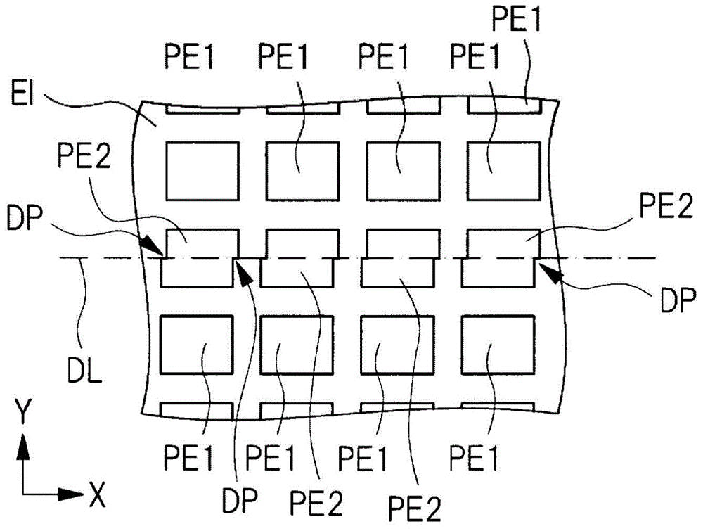
[0159] Figure 14 Shown is a plan layout diagram of a semiconductor device in this embodiment mode. Figure 14 and Figure 4 Similarly, among the plurality of pixels arranged in the pixel array section of the solid-state image sensor, the pixel PE2 that coincides with the boundary line DL in planar view is shown. The configuration of the solid-state image sensor in this embodiment is almost the same as that of the solid-state image sensor in the first embodiment, but Figure 14 In the present invention, the distance between the photodiodes PD1 and PD2 in the pixel PE2 is large, which is different from the first embodiment.
[0160] Specifically, compared with the first embodiment, the formation positions of the photo...
no. 3 Embodiment approach
[0177] In this embodiment mode, the distance between the photodiodes arranged in the pixel is increased and the area of the photodiodes is reduced.
[0178] Figure 16 Shown is a plan layout diagram of a semiconductor device in this embodiment mode. Figure 16 and Figure 4 Similarly, among the plurality of pixels arranged on the pixel array portion of the solid-state image sensor, the pixel PE2 that coincides with the boundary line DL in planar view is shown. The structure of the solid-state image sensor in this embodiment is almost the same as that of the second embodiment, including that the distance between the photodiodes PD1 and PD2 in the pixel PE2 is relatively large. Figure 16 The photodiodes PD1 and PD2 in the middle pixel PE2 are different from the second embodiment in that the area of each of the photodiodes PD1 and PD2 is small.
[0179] That is to say, in the second embodiment, by shifting the formation positions of the photodiodes PD1 and PD2 in the pixe...
PUM
 Abstract
Description
Claims
Application Information