Mass-production apparatus capable of fast improving photoinduced degradation of a P-type crystalline silicon cell and using method thereof
A technology of crystalline silicon cells and light-induced attenuation, applied in the field of solar cells, can solve problems such as difficulties in large-scale mass production, increased production costs, and decreased cell efficiency, and achieve improved processing efficiency and product quality, consistent airflow temperature, and light-induced attenuation. The effect of attenuation improvement
- Summary
- Abstract
- Description
- Claims
- Application Information
AI Technical Summary
Problems solved by technology
Method used
Image
Examples
Embodiment 1
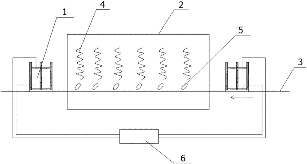
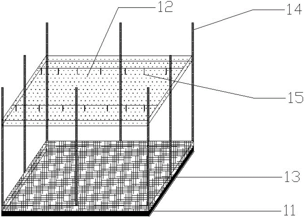
[0036] Stack 100 pieces of p-type monocrystalline silicon solar cells according to the order of all the fronts up and put them into the silicon wafer carrying box, and use DC power supply to energize, and the current density is set to 1000mA / cm 2 , keep the temperature of the incubator at 250°C, set the speed of the conveyor belt so that the passage time of the silicon wafer carrier box in the incubator is 15 minutes, and take out the cells after cooling naturally. The treated cells were compared with the same batch of untreated cells, and the results are as follows:
[0037]
Embodiment 2
[0039] Stack 200 pieces of p-type polycrystalline silicon solar cells according to the order of all the fronts up and put them into the silicon wafer carrying box, and use DC power supply to energize, and the current density is set to 3000mA / cm 2 , keep the temperature of the incubator at 375°C, set the speed of the conveyor belt so that the passage time of the silicon wafer carrier box in the incubator is 8 minutes, and take out the cells after cooling naturally. The treated cells were compared with the same batch of untreated cells, and the results are as follows:
[0040]
Embodiment 3
[0042] Stack 55 pieces of p-type monocrystalline silicon solar cells according to the order of all the fronts up and put them into the silicon wafer carrying box, and electrify with a pulse power supply, and the current density is set to 501mA / cm 2 , keep the temperature of the incubator at 230°C, set the speed of the conveyor belt so that the silicon wafer carrying box passes through the incubator for 20 minutes, and take out the cells after cooling naturally. The treated cells were compared with the same batch of untreated cells, and the results are as follows:
[0043]
PUM
 Abstract
Description
Claims
Application Information


