Field effect transistor resistant to single-particle radiation and preparation method thereof

A technology for field effect transistors and anti-single event radiation, which is applied in semiconductor/solid-state device manufacturing, semiconductor devices, electrical components, etc., and can solve problems such as limitations

Inactive Publication Date: 2015-12-16
PEKING UNIV
View PDF2 Cites 5 Cited by
  • Summary
  • Abstract
  • Description
  • Claims
  • Application Information

AI Technical Summary

Problems solved by technology

In addition, the sensitivity of devices and circuits to single-event radiation can also be reduced by increasing the gate length and gate width of the MOSFET, but since the gate length and gate width of the device are also important parameters affecting conventional performance, and increasing the gate The length and gate width are contrary to the improvement of integration, so the use of this method is limited

Method used


Image

  • Field effect transistor resistant to single-particle radiation and preparation method thereof
  • Field effect transistor resistant to single-particle radiation and preparation method thereof
  • Field effect transistor resistant to single-particle radiation and preparation method thereof

Examples


Embodiment Construction

[0030] The present invention will be further described through the embodiments below in conjunction with the accompanying drawings.

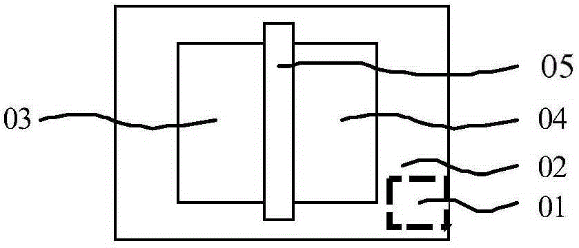
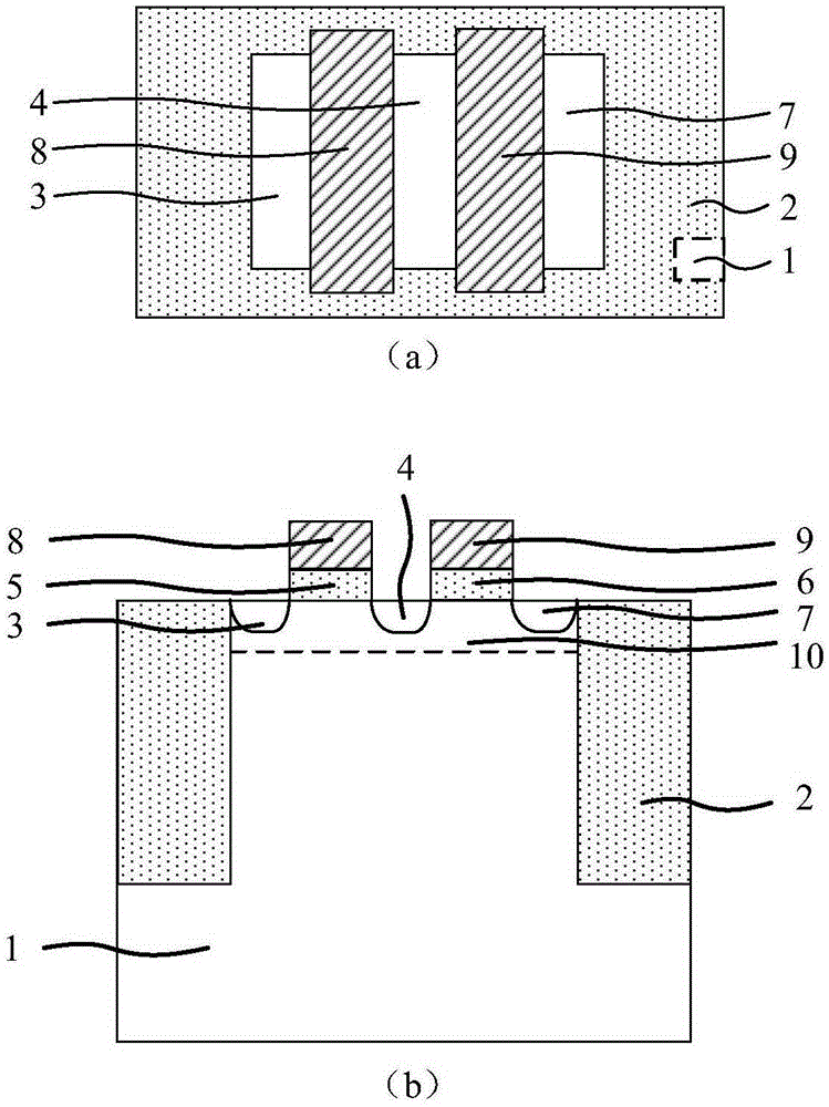
[0031] Such as figure 2 As shown, the anti-single event radiation field effect transistor of this embodiment includes: a substrate 1, a shallow trench isolation region 2, a doped region 10, a source region 3, a drain region 4, a redundant electrode region 7, and a main gate dielectric 5 , a redundant gate dielectric 6, a main gate 8 and a redundant gate 9; wherein, the doped region 10 is formed on the substrate 1; the shallow trench isolation region 2 surrounds the doped region 10 and is embedded in the substrate 1; Inside the doped region 2 are a source region 3, a drain region 4, and a redundant electrode region 7 that are isolated from each other in sequence; a main gate dielectric 5 is formed on the doped region 10 and between the source region 3 and the drain region 4; A redundant gate dielectric 6 is formed above the region 10 and betwee...


PUM


Abstract

The invention discloses a field effect transistor (FET) resistant to single-particle radiation and a preparation method thereof. The FET comprises a substrate, a shallow trench isolation region, a doped region, a source region, a drain region, a redundancy electrode region, a main transistor gate dielectric, a redundancy gate dielectric, a main transistor gate electrode, and a redundancy gate electrode. The preparation method belongs to a layout-level design reinforcing method and may suppress the sensitivity, to single-particle radiation, of the MOSFET at a source generating a transient pulse to a certain extent. Based on a charge sharing principle of an irradiation effect, the redundancy electrode region/a substrate pn junction is formed around a sensitive pn junction so that the operation of the MOSFET is not influenced when no radiation is generated and charges generated by a radiation ionization effect can be shared and collected when radiation is generated. Thus, the collected charges of the protected sensitive pn junction are reduced. In addition, compared with a design reinforcing method using high-density body contact/trap contact, the method of the invention requires small total layout area and achieves a higher integrated level.

Description

technical field [0001] The invention relates to the field of radiation effects of semiconductor integrated circuits, in particular to a field-effect transistor resistant to single-event radiation and a preparation method thereof. Background technique [0002] Metal-oxide-semiconductor field-effect transistor MOSFETs are widely used in integrated circuits, but MOSFETs are susceptible to single-event radiation effects in space or ground environments. When heavy ions, protons, neutrons, electrons and other particles of a certain energy are incident on the MOSFET, due to the ionization effect of the particles, a large number of electron-hole pairs will be generated in the semiconductor material. When there is a potential distribution in the semiconductor material, the electron-hole pairs will move under the action of the electric field and be absorbed by the anode and cathode respectively, forming a transient current or voltage pulse. A transient pulse will propagate within the...

Claims


Application Information

Patent Timeline
Patent Type & Authority Applications(China)
IPC IPC(8): H01L29/423H01L29/06H01L29/78H01L21/336
CPCH01L29/42316H01L29/0603H01L29/0684H01L29/66484H01L29/783
Inventor 黄如武唯康安霞刘静静阙陶张兴
Owner PEKING UNIV
Why Eureka
Try Eureka