
Nitride light emitting diode (LED) based on stress controlled electroplating and substrate transferring and fabrication method thereof

A technology of stress control and substrate transfer, applied in circuits, electrical components, semiconductor devices, etc., can solve problems such as high temperature, epitaxial layer cracking, and increased epitaxial layer damage, and achieve the goals of preventing leakage, ensuring compactness, and ensuring integrity Effect

Inactive Publication Date: 2015-12-16
SOUTH CHINA UNIV OF TECH
View PDF2 Cites 14 Cited by
  • Summary
  • Abstract
  • Description
  • Claims
  • Application Information

AI Technical Summary

Problems solved by technology

The main method of removing the sapphire substrate is laser lift-off, but the instantaneous high temperature will be generated during the laser lift-off process, which will affect the quality of the epitaxial layer, resulting in a decrease in luminous efficiency, and in more serious cases, the epitaxial layer may be broken
At present, LED epitaxial wafers with patterned sapphire substrates are mainly used in industrialization. Due to the influence of scattering, laser lift-off method will require more laser energy to process patterned substrates, and the damage to the epitaxial layer will increase accordingly.

Method used


Image

  • Nitride light emitting diode (LED) based on stress controlled electroplating and substrate transferring and fabrication method thereof
  • Nitride light emitting diode (LED) based on stress controlled electroplating and substrate transferring and fabrication method thereof
  • Nitride light emitting diode (LED) based on stress controlled electroplating and substrate transferring and fabrication method thereof

Examples


Embodiment

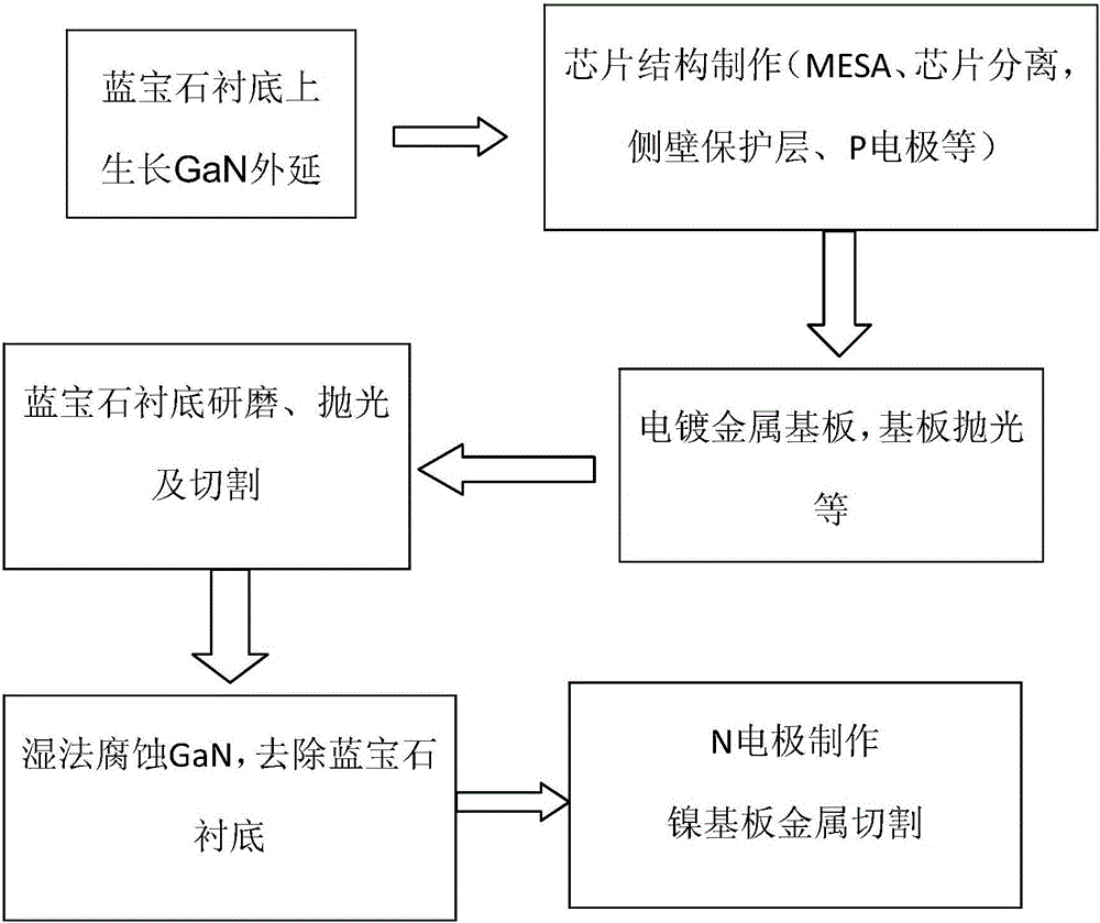
[0057] Such as figure 1 As shown in Fig. 2, the method for preparing a vertical structure LED by peeling off the sapphire sapphire substrate of the present invention by wet etching, the specific preparation process is as follows:

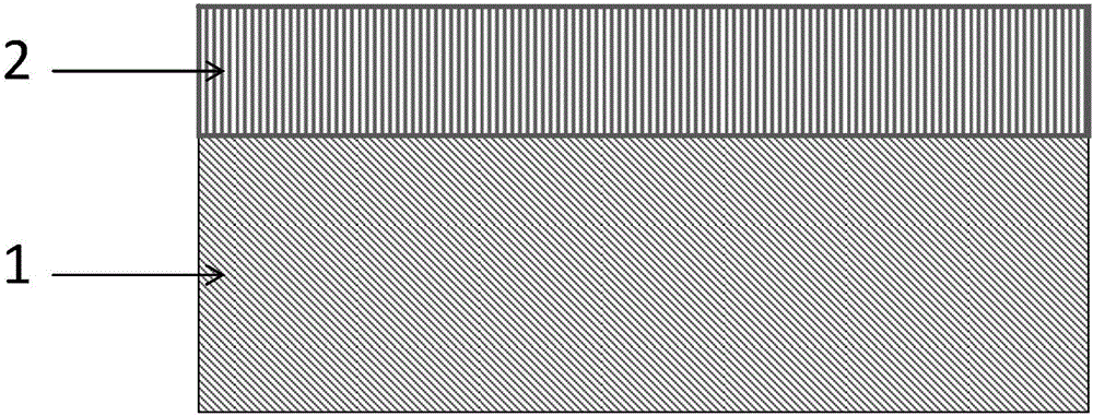
[0058] [1] Using an MOCVD epitaxial growth system, a GaN epitaxial layer 2 is grown on a c-plane patterned sapphire substrate 1, and the epitaxial layers are grown sequentially in the order of GaN buffer layer, u-GaN layer, n-GaN layer, and multi-quantum well layer (MQW) and p-GaN layer, the thickness of the entire GaN-based epitaxial layer should be greater than 6 μm. Such as Figure 2a shown.

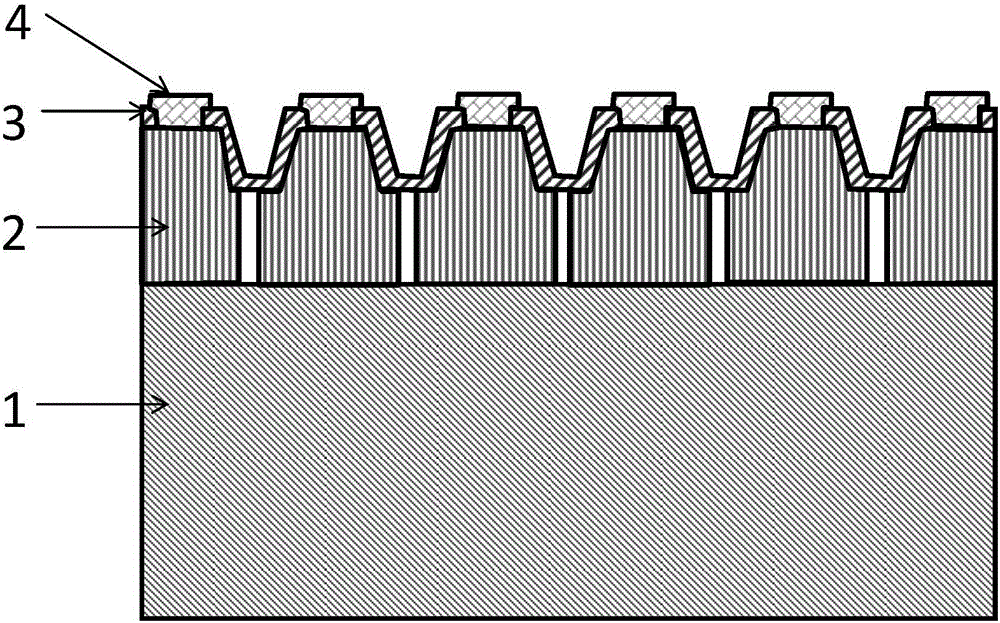
[0059] [2] Through photolithography and inductively coupled plasma dry etching process, the gallium nitride epitaxial layer (ie GaN epitaxial layer 2) on the sapphire substrate is etched to a depth of 3.2 μm, and its thickness is controlled by adjusting the photolithography conditions. The inclination angle of the side wall is 40-70 degrees.

[0060] [3...


PUM

PropertyMeasurementUnit
Thicknessaaaaaaaaaa
Thicknessaaaaaaaaaa
Thicknessaaaaaaaaaa

Abstract

The invention provides a nitride light emitting diode (LED) based on stress controlled electroplating and substrate transferring and a fabrication method thereof. A method for stripping a sapphire substrate through wet etching can be used for fabricating a vertical structure LED. The separation of the sapphire substrate and a gallium nitride epitaxial layer can be achieved by key steps of cutting the gallium nitride epitaxial layer, cleaning the gallium nitride epitaxial by using a hot acid, releasing gallium nitride stress, electroplating a stress-free nickel substrate, polishing a metal substrate, fabricating an inclined gallium nitride side wall, a metal sacrificial layer and a side wall protection layer, polishing the sapphire substrate, cutting in one time, corroding an N-polarity surface of the gallium nitride and the like. By the method, the crystal quality of a GaN active layer cannot be affected, and thus, the luminous efficiency of the vertical structure LED can be guaranteed.

Description

technical field [0001] The invention belongs to the technical field of semiconductor lighting, relates to a gallium nitride-based vertical structure LED chip and a preparation method thereof, and is especially suitable for the field of white light lighting. Background technique [0002] Light-emitting diodes (LEDs) are considered to be the fourth generation of light sources in human history after incandescent lamps, fluorescent lamps and high-intensity discharge lamps. Gallium nitride (GaN) material, as a typical representative of the third-generation semiconductor material, has the advantages of large band gap, good thermal and chemical stability, small dielectric constant, high thermal conductivity, and radiation resistance, and it belongs to Materials with a direct bandgap structure have extremely high radiative recombination efficiency, so they are widely used in the preparation of light-emitting devices. [0003] The substrates used for the epitaxial growth of GaN ma...

Claims


Application Information

Patent Timeline
IPC IPC(8): H01L33/32H01L33/00
CPCH01L33/00H01L33/32
Inventor 胡晓龙王洪蔡镇准齐赵毅
Owner SOUTH CHINA UNIV OF TECH
Learn More