
A method for directly depositing nano-graphene to suppress secondary electron emission

A technology of secondary electron emission and nano-graphene, which is applied in the direction of gaseous chemical plating, metal material coating process, coating, etc., can solve the problems of poor stability and complicated process of suppressing electron emission, and achieve the reduction of secondary electron emission Coefficient, process is simple and convenient, easy to achieve the effect

Active Publication Date: 2017-12-22
XIAN INSTITUE OF SPACE RADIO TECH
View PDF3 Cites 0 Cited by
  • Summary
  • Abstract
  • Description
  • Claims
  • Application Information

AI Technical Summary

Problems solved by technology

However, the existing methods for suppressing secondary electron emission are complicated in technology and have poor stability in suppressing electron emission.

Method used


Image

  • A method for directly depositing nano-graphene to suppress secondary electron emission
  • A method for directly depositing nano-graphene to suppress secondary electron emission
  • A method for directly depositing nano-graphene to suppress secondary electron emission

Examples


Embodiment 1

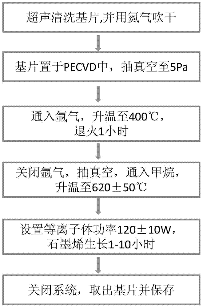
[0044] The nano-graphene film is directly grown on the silver and copper substrates by plasma-enhanced chemical vapor deposition, so as to reduce the secondary electron emission coefficient. The method specifically includes the following steps:

[0045](1) The silver and copper substrates with a length, width and thickness of 15.0mm×12.0mm×0.3mm were ultrasonically cleaned with acetone and alcohol for 30 minutes, respectively, to remove the surface adsorption of the substrate, and blow dry with nitrogen;

[0046] (2) Place the substrate in a remote plasma-enhanced chemical vapor deposition system (PECVD), turn on the mechanical pump, and evacuate to 5Pa, and then keep the vacuum mechanical pump working normally;

[0047] (3) Argon gas with a flow rate of 50 sccm is introduced, the temperature is slowly raised from room temperature to 400° C. over 20 minutes, and annealed at 400° C. for 1 hour;

[0048] (4) Turn off the argon gas, evacuate to below 5Pa, introduce 30sccm methan...

Embodiment 2

[0053] The concrete method of growing nano-graphene film on silver, copper substrate is the same as embodiment 1, and difference is that the control graphene growth time is 10 hours.

[0054] In the experiment, the secondary electron emission coefficient of the substrate is studied by the current method. The measured secondary electron emission coefficient of the metal copper substrate is 2.16-2.39, and the secondary electron emission coefficient of the silver substrate is 1.97-2.13. The natural graphite material and high orientation The secondary electron emission coefficient of pyrolytic graphite (HOPG) is about 1.28-1.32. Control the graphene growth time for 10 hours, after the nano-graphene material grows on the surface of the copper substrate, its secondary electron emission coefficient drops to 1.04, and the drop can reach 55%. When the secondary electron emission coefficient is 1, the first incident energy point is from 40eV increased to 270eV. After growing nanographe...

Embodiment 3

[0056] The specific method of growing nano-graphene film on copper substrate is the same as embodiment 1, the difference is that the control of graphene growth time is 1-10 hour change.

[0057] With different growth times, the growth thickness of graphene on the substrate surface is different, and its ability to inhibit secondary electron emission is also different. The longer the life time, the greater the thickness of the surface nano-graphene. The graphene growth time on the copper substrate corresponds to the secondary electron emission coefficient as follows: Figure 5 As shown, the experimental results show that different secondary electron emission suppression effects can be achieved by controlling the growth time.


PUM

PropertyMeasurementUnit
thicknessaaaaaaaaaa

Abstract

The invention relates to a method for directly depositing nano-graphene to suppress secondary electron emission. The method applies plasma-enhanced chemical vapor deposition nano-graphene technology to the field of suppressing secondary electron emission, and improves and optimizes the process Designed to realize the growth of nano-graphene film with controllable thickness on the surface of the metal substrate, which can reduce the secondary electron emission coefficient to less than 1.1. At the same time, the process stability is high, and the substrate secondary electron emission The variation of the coefficient is less than 10%, and the invention has good application prospects in solving micro-discharge effects of microwave components and electron clouds of particle accelerators.

Description

technical field [0001] The invention relates to a method for directly depositing nano-graphene to suppress secondary electron emission, and belongs to the technical field of vacuum electronics secondary electron emission suppression. Background technique [0002] Secondary electron emission refers to the phenomenon that when primary electrons with a certain energy are incident on the sample surface, secondary electrons will be excited from the sample surface. The ratio of the number of secondary electrons to the number of primary electrons is called the secondary electron emission coefficient, which numerically means the number of secondary electrons that can be produced by an average single incident electron. The secondary electron emission depends on many factors, such as the atomic number of the material, the lattice structure, the surface morphology, and the energy and angle of the incident electrons. [0003] In vacuum electronic devices, secondary electron emission is...

Claims


Application Information

Patent Timeline
Patent Type & Authority Patents(China)
IPC IPC(8): C23C16/26C23C16/513
Inventor 谢贵柏崔万照杨晶胡天存
Owner XIAN INSTITUE OF SPACE RADIO TECH
Learn More