Nanowire huge piezoresistive characteristic measuring device and manufacturing method thereof

A measurement device and nanowire technology, applied in the field of micro-nano electromechanical systems, can solve problems such as influence and reduce measurement accuracy, and achieve the effects of easy research, improved accuracy, and guaranteed consistency

Inactive Publication Date: 2016-01-06
NANJING UNIV OF INFORMATION SCI & TECH
View PDF4 Cites 6 Cited by
  • Summary
  • Abstract
  • Description
  • Claims
  • Application Information

AI Technical Summary

Problems solved by technology

[0005] It is worth noting that due to temperature drift, the sensitivity and stability of semiconductor giant piezoresistive sensors will be affected to a certain extent, and the measurement accuracy will be reduced. Therefore, the temperature drift effect of semiconductor piezoresistive sensors used in various temperature environments needs to be considered. However, there are few studies on the temperature characteristics of the piezoresistive coefficient of nanowires, so there is an urgent need for related measurement and research methods

Method used


Image

  • Nanowire huge piezoresistive characteristic measuring device and manufacturing method thereof
  • Nanowire huge piezoresistive characteristic measuring device and manufacturing method thereof
  • Nanowire huge piezoresistive characteristic measuring device and manufacturing method thereof

Examples


preparation example Construction

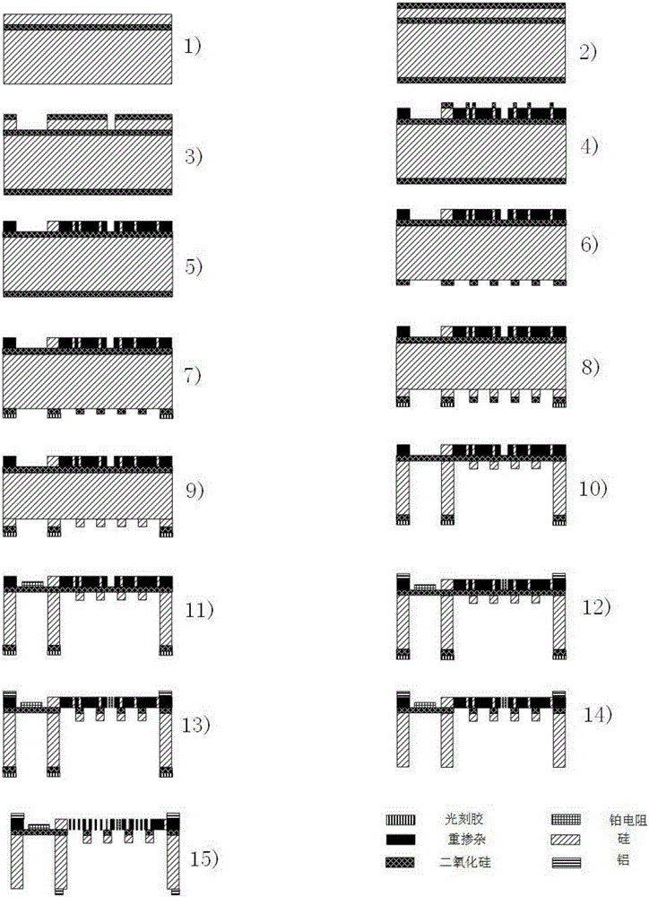
[0056] Such as image 3 As shown, a preparation method of a nanowire giant piezoresistive characteristic measuring device, the specific steps of the method:

[0057] 1) Choose an SOI silicon wafer with a top silicon layer of 25 μm, a buried oxide layer of 2 μm, and a bottom silicon layer of 300 μm, and place the silicon wafer in a mixed solution of acetone, hydrogen peroxide, and concentrated sulfuric acid for ultrasonic cleaning, and then repeatedly clean it with deionized water; then Put the cleaned silicon chip into the diluted HF solution to react to remove the oxide layer on the surface of the silicon chip;

[0058] 2) Deposit 1 μm SiO on the top and bottom silicon of the SOI wafer by LPCVD technology 2 oxide layer;

[0059] 3) Etch the top layer SiO by RIE (reactive ion etching) technology 2 The oxide layer forms the platinum resistance area; the platinum resistance area is etched by DRIE (deep reactive ion etching) technology;

[0060] 4) Etching the top layer SiO b...

Embodiment 1

[0075] Example 1: Silicon nanowires with silver

[0076] The experimental process for the preparation of Si nanowires is as follows: firstly, 2% HF solution (HF:H 2 O=1:50) to clean the Si wafer for 3 minutes to remove the natural oxide layer on the surface of the Si wafer; then, put the silicon wafer into a mixed solution of acetone, hydrogen peroxide and concentrated sulfuric acid for ultrasonic cleaning, and then deionized water Repeated cleaning; then use a vacuum evaporation coating machine to evaporate high-purity Au, and deposit a certain thickness of metal catalyst on the surface of the Si substrate; finally, place the sample of the deposited metal catalyst in the quartz tube of the automatic temperature-controlled tubular oxidation furnace, Under the protective atmosphere with a temperature of 800-1100° C. and a certain flow rate, high-temperature annealing is performed to grow Si nanowires. Treat the oxide film on the nanowires with hydrofluoric acid, passivate the ...

Embodiment 2

[0077] Example 2: SiGe Radial Heterojunction Nanowires

[0078] Gold nanoclusters were deposited on an oxidized silicon wafer and placed in a quartz tube furnace. At 450°C, using silane as a precursor gas, the silicon nanowire core grows at a growth rate of about 2 μm / min in the axial direction, and then uses silane and 100 ppm helium diborane as a precursor gas to deposit a p-type silicon shell, And at a radial growth rate of 10 nm / min. Then, under the condition of 380°C, the germanium nanowires were grown at an axial growth rate of 0.72um / min in 10% of the relevant argon gas, while the germanium shell was grown in the furnace at a growth rate of 10nm / min by changing the position and environment of the growth substrate. Radial velocity deposition. Nanowires of various core-shell structures, such as Si / Ge, Ge / Si, or Si / Ge / Si, Ge / Si / Ge, etc., can be completed by repeating the above process. Its process flow chart is as Figure 4 .


PUM


Abstract

The invention discloses a nanowire huge piezoresistive characteristic measuring device and a manufacturing method thereof. The nanowire huge piezoresistive characteristic measuring device comprises a nanowire, a platinum resistor temperature sensor, an electrothermal actuator, a displacement sensor based on capacitance measurement, electrodes and a load sensor based on capacitance measurement. The platinum resistor temperature sensor, the electrothermal actuator, the displacement sensor based on capacitance measurement and the load sensor based on capacitance measurement are connected in sequence. The number of the electrodes is four. The four electrodes are arranged between the displacement sensor based on capacitance measurement and the load sensor based on capacitance measurement. The nanowire is arranged between two horizontally-arranged electrodes. By adopting the nanowire huge piezoresistive characteristic measuring device and the manufacturing method thereof, machinery characteristics and electrical characteristics of the nanowire are measured simultaneously, and the representation of a piezoresistive coefficient is realized; in addition, the nanowire huge piezoresistive characteristic measuring device is applicable to different kinds of measurement samples.

Description

technical field [0001] The invention relates to a nanowire giant piezoresistive characteristic measuring device and a manufacturing method thereof, and belongs to the technical field of micro-nano electromechanical systems. Background technique [0002] As a typical one-dimensional semiconductor nanomaterial, nanowires not only have the characteristics of general nanomaterials, but also have the characteristics of being compatible with modern large-scale integrated circuit technology, easy to be prepared in large quantities, and convenient for surface modification. Due to the semiconductor properties of nanowires showing unique electrical, mechanical, thermal and chemical properties, its research scope and application fields cover many fields from chemistry, physics, biology, environmental sensors, field effect transistors and logic circuits. In addition, silicon nanowires also show field emission, thermal conductivity, visible photoluminescence and quantum confinement effec...

Claims


Application Information

Patent Timeline
Patent Type & Authority Applications(China)
IPC IPC(8): G01R27/02G01R3/00B82Y15/00
CPCB82Y15/00G01R3/00G01R27/02
Inventor 张加宏赵阳李敏杨敏
Owner NANJING UNIV OF INFORMATION SCI & TECH
Why Eureka
Try Eureka