Composite electrode materials and their uses
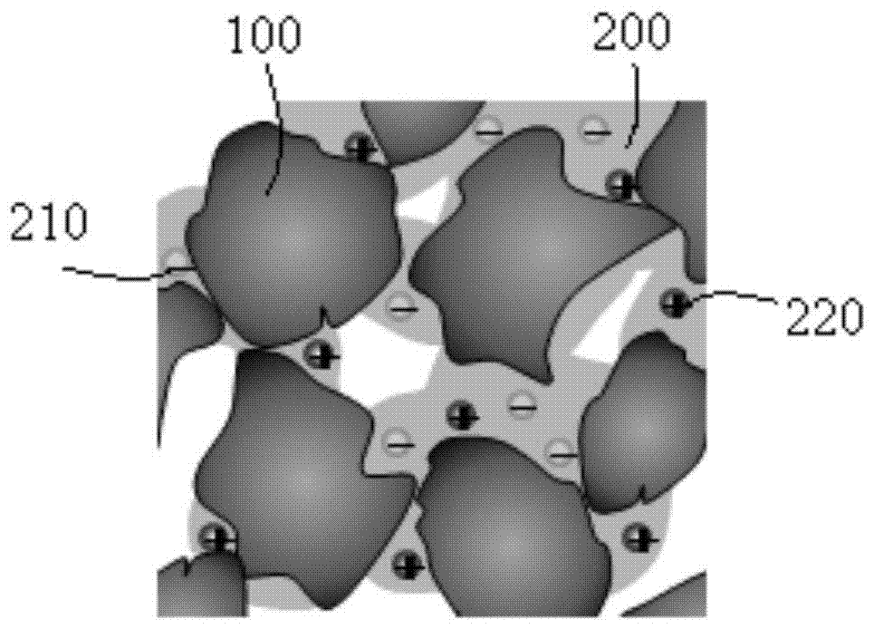
A composite electrode and active material technology, applied in the direction of hybrid capacitor electrodes, can solve the problems of limiting the application of three-dimensional electrode structures, the capacitance of solid electrolytes to be studied, etc., to solve the problem of small electrode thickness, higher capacitance, and high energy storage density Effect
- Summary
- Abstract
- Description
- Claims
- Application Information
AI Technical Summary
Problems solved by technology
Method used
Image
Examples
Embodiment 1
[0086] In this embodiment, activated carbon is used as the electrode active material, phosphoric acid is used as the ionic compound providing electrolyte anions and cations, and PVA (polyvinyl alcohol) is used as the ion-conducting matrix. The specific preparation process is as follows:
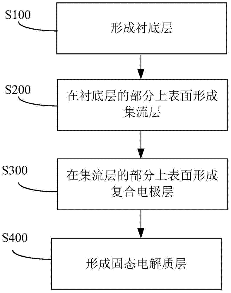
[0087] (1) A substrate layer is formed on a silicon wafer, and a silicon nitride film with a thickness of about 100 nanometers is deposited on the silicon wafer by a low pressure vapor deposition (LPCVD) method.
[0088] (2) Photolithography is carried out on the substrate layer, and then a Cr / Au metal current collecting layer is vapor-deposited thereon. The thickness of the current collecting layer is 100 nanometers, and then peeled off to remove the redundant metal layer;
[0089] (3) Utilize the photoresist SU-8 to directly realize the diaphragm layer with the interdigitated groove structure through the photolithography method in the micromachining technology, and the thickness of the diaph...
Embodiment 2
[0094] In this embodiment, graphene is used as the electrode active material, sulfuric acid is used as the ionic compound providing electrolyte anions and cations, and PEO (polyethylene oxide) is used as the ion-conducting matrix. The specific preparation process is as follows:
[0095] (1) A substrate layer is formed on a silicon wafer, and a silicon nitride film with a thickness of about 100 nanometers is deposited on the silicon wafer by a low-pressure vapor deposition (LPCVD) method;
[0096] (2) Photolithography is carried out on the substrate layer, and then a Cr / Au metal current collecting layer is vapor-deposited thereon. The thickness of the current collecting layer is 100 nanometers, and then peeled off to remove the redundant metal layer;
[0097] (3) Utilize the photoresist SU-8 to directly realize the diaphragm layer with the interdigitated groove structure through the photolithography method in the micromachining technology, and the thickness of the diaphragm laye...
PUM
| Property | Measurement | Unit |
|---|---|---|
| thickness | aaaaa | aaaaa |
| thickness | aaaaa | aaaaa |
Abstract
Description
Claims
Application Information


