Preparation method of ultraviolet and visible coexisting electroluminescent device

An electroluminescent device, ultraviolet technology, applied in the direction of electrical components, semiconductor devices, circuits, etc., can solve the problems of energy level matching and structural design that increase the difficulty of preparation, affect the luminous efficiency of the device, and increase the difficulty of device preparation, etc., to achieve convenient batch production Simple production, high repeatability, easy-to-achieve effects

Active Publication Date: 2016-02-17
AVIC BEIJING INST OF AERONAUTICAL MATERIALS
View PDF3 Cites 3 Cited by
  • Summary
  • Abstract
  • Description
  • Claims
  • Application Information

AI Technical Summary

Problems solved by technology

This greatly increases the difficulty of device preparation, because the superposition of multiple light-emitting layer materials undoubtedly greatly increases the difficulty of preparation in terms of energy level matching and structural design.
At the same time, this also affects the luminous efficiency of the device, because the light emitted by the luminescent material at the bottom will greatly reduce the efficiency when it penetrates the upper luminescent layer.

Method used


Image

  • Preparation method of ultraviolet and visible coexisting electroluminescent device
  • Preparation method of ultraviolet and visible coexisting electroluminescent device
  • Preparation method of ultraviolet and visible coexisting electroluminescent device

Examples


preparation example Construction

[0019] The invention provides a method for preparing the above-mentioned electroluminescent device, comprising:

[0020] (1) The CdZnO thin film is deposited on the substrate by sputtering, wherein the target used for depositing the CdZnO thin film is a CdZnO ceramic target, and the Cd doping amount in the CdZnO ceramic target is 60% by molar content, and the substrate heating temperature is 400 ~500°C, the sputtering power is 120W, the sputtering time is 1 hour, and the air pressure is 4Pa. Then put the film into a tube furnace under the protection of an inert atmosphere for heat treatment, the heat treatment temperature is 600-800°C, and the heat treatment time is 10-60 minutes;

[0021] (2) The MgO film is prepared on the CdZnO film by the sol-gel method, and then the film is subjected to heat treatment, the heat treatment temperature is 300-400° C., and the heat treatment time is 1-2 hours. ;

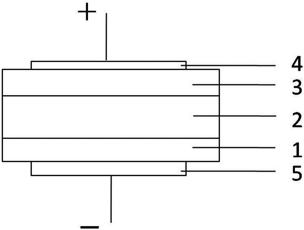
[0022] (3) A translucent Au electrode is deposited on the MgO film by sputter...

Embodiment 1

[0025] 1) Clean N-type , with a resistivity of 0.005 ohm cm and a size of 15×15mm 2 , a silicon wafer with a thickness of 675 microns;

[0026] 2) Deposit CdZnO film on Si substrate by radio frequency sputtering, substrate temperature is 400°C; sputtering power is 120W, Ar, O 2 The flow rate is 30:15, the air pressure is 4Pa, the sputtering is for 1 hour, and the thickness is about 400nm. After deposition in N 2 Heat treatment at 600°C for 1 hour in a tube furnace under atmosphere;

[0027] 3) Spin-coat a layer of MgO film on the CdZnO film, dry at 100°C for 10 minutes, and heat-treat at 300°C for 2 hours in air;

[0028] 4) A translucent Au electrode 4 about 20 nm thick is sputtered on the MgO film, and an Au electrode (ohmic contact electrode 5 ) about 100 nm thick is sputtered on the backside of the silicon substrate. The sputtering power is 45W, the Ar flow rate is 20, the air pressure is 5Pa, and the substrate temperature is 150°C. The front electrode was sputtered f...

Embodiment 2

[0031] 1) Clean N-type , with a resistivity of 50 ohm cm and a size of 15×15mm 2 , a silicon wafer with a thickness of 675 microns;

[0032] 2) Deposit CdZnO film on Si substrate by radio frequency sputtering, substrate temperature is 500°C; sputtering power is 120W, Ar, O 2 The flow rate is 30:15, the air pressure is 4Pa, the sputtering is for 1 hour, and the thickness is about 400nm. After deposition in N 2 Heat treatment at 800°C for 10 minutes in a tube furnace under atmosphere;

[0033] 3) Spin-coat a layer of MgO film on the CdZnO film, dry at 100°C for 10 minutes, and heat-treat at 400°C for 1 hour in air;

[0034] 4) A translucent Au electrode 4 about 20 nm thick is sputtered on the MgO film, and an Au electrode (ohmic contact electrode 5 ) about 100 nm thick is sputtered on the backside of the silicon substrate. The sputtering power is 45W, the Ar flow rate is 20, the air pressure is 5Pa, and the substrate temperature is 150°C. The front electrode was sputtered f...


PUM

PropertyMeasurementUnit
electrical resistivityaaaaaaaaaa

Abstract

The invention belongs to the field of photoelectric devices, relates to a preparation method of an ultraviolet and visible coexisting electroluminescent device, and particularly relates to a preparation method of an ultraviolet and visible coexisting electroluminescent device with an Au/MgO/CdZnO/SiMIS structure. The device comprises a substrate. A CdZnO thin film, a MgO thin film and an Au electrode are deposited on the front surface of the substrate from the bottom to the top in turn. An ohmic contact electrode is deposited on the back surface of the substrate. According to the device, a ZnO and CdZnO coexisting thin film luminescent layer is obtained by performing thermal treatment on the sputtering CdZnO thin film, and the thin film is enabled to emit electroluminescence arranged in an ultraviolet and visible region under certain forward bias voltage (the substrate is connected with negative voltage). Besides, the structure and the realization mode of the device are simple, and the preparation technology and the used equipment are compatible with the current mature silicon device technology.

Description

technical field [0001] The invention belongs to the field of optoelectronic devices, and relates to a method for preparing an electroluminescent device with both ultraviolet and visible light, in particular to a method for preparing an electroluminescent device with an Au / MgO / CdZnO / SiMIS structure with both ultraviolet and visible light. Background technique [0002] Zinc oxide (ZnO) is an important direct wide bandgap semiconductor material with a bandgap width of 3.37ev at room temperature. Because of its abundant raw materials, low cost, non-toxic and pollution-free, and high room temperature exciton binding energy (about 60meV), it is considered to be a new generation of short-wavelength light-emitting materials that may replace gallium nitride (GaN). It has attractive application prospects in the fields of semiconductor lighting, flat display and ultraviolet light detection. [0003] In recent years, with the development of ultraviolet and white LED technology, people'...

Claims


Application Information

Patent Timeline
Patent Type & Authority Applications(China)
IPC IPC(8): H01L33/00H01L33/28
CPCH01L33/0083H01L33/0095H01L33/28
Inventor 田野罗飞刘大博祁洪飞
Owner AVIC BEIJING INST OF AERONAUTICAL MATERIALS
Why Eureka
Try Eureka