

Low-temperature polycrystalline silicon thin film transistor and preparation method thereof
一种薄膜晶体管、低温多晶硅的技术,应用在晶体管、半导体/固态器件制造、电固体器件等方向,能够解决多晶硅晶粒尺寸小、多晶硅实际应用限制等问题,达到提升驱动效率的效果
- Summary
- Abstract
- Description
- Claims
- Application Information
AI Technical Summary
Problems solved by technology
Method used
Image

Examples
Embodiment 1
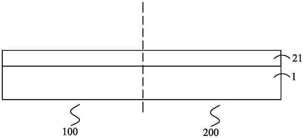
[0056] This embodiment provides a low temperature polysilicon thin film transistor, the thin film transistor includes a pixel thin film transistor and a driving thin film transistor, and the preparation method of the low temperature polysilicon thin film transistor is as follows:
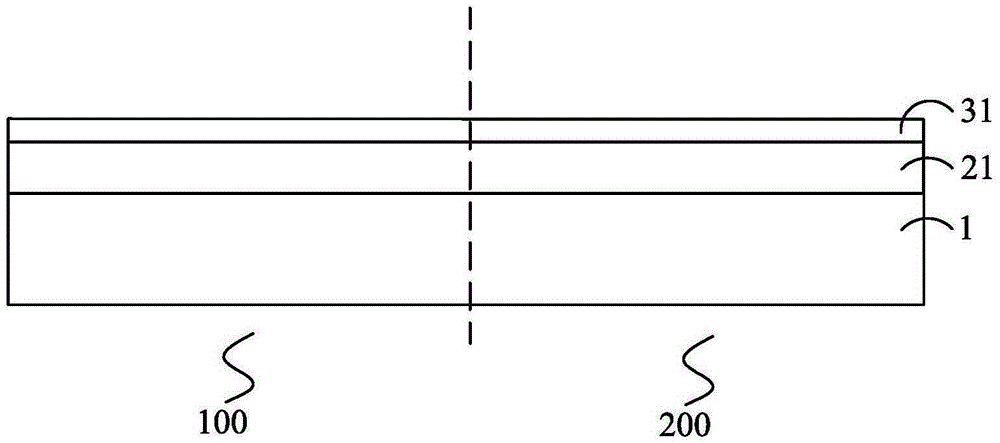
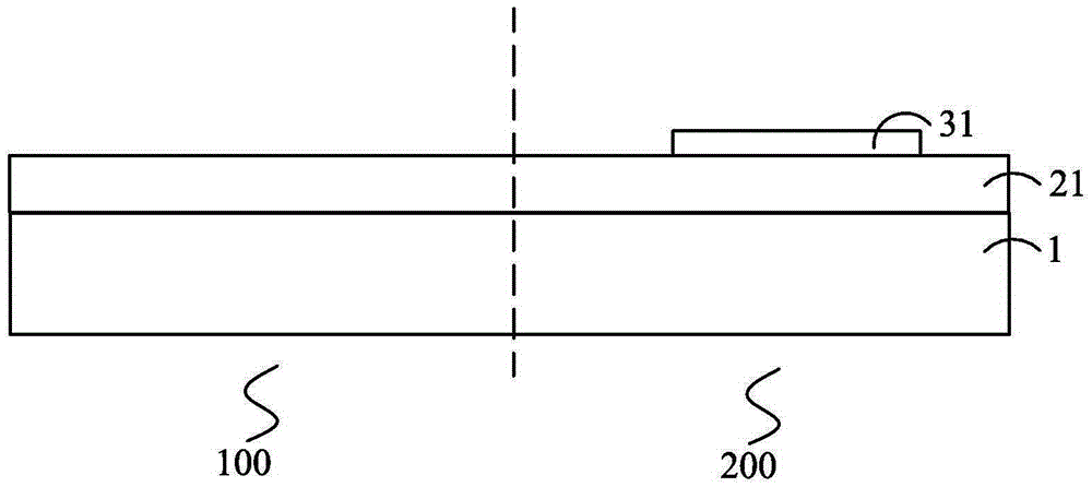
[0057] like figure 1 As shown, a glass substrate 1 is provided, and the glass substrate 1 includes a pixel area 100 on the left side and a peripheral driving area 200 on the right side. A pixel thin film transistor is formed in the pixel area 100 , and a driving thin film transistor as a driving unit is formed in the peripheral driving area 200 . Use chemical vapor deposition (CVD, Chemical VaporDeposition) method to form first buffer layer 21 on glass substrate 1, this first buffer layer is silicon nitride layer; Then, as figure 2 As shown, a metal molybdenum layer 31 is deposited and formed on the first buffer layer 21 as a reflective layer by using a chemical vapor deposition method, and a pho...
Embodiment 2
[0065] This embodiment provides a low temperature polysilicon thin film transistor, the thin film transistor includes a pixel thin film transistor and a driving thin film transistor, and the preparation method of the low temperature polysilicon thin film transistor is as follows:
[0066] like Figure 12 As shown, a glass substrate 1 is provided, and the glass substrate 1 includes a pixel area 100 on the left side and a peripheral driving area 200 on the right side. A pixel thin film transistor is formed in the pixel area 100 , and a driving thin film transistor as a driving unit is formed in the peripheral driving area 200 . A first buffer layer 21 and a second buffer layer 22 are sequentially deposited on the glass substrate 1 using a chemical vapor deposition method, the first buffer layer is a silicon nitride layer, and the second buffer layer is a silicon dioxide layer; then, as Figure 13 As shown, an aluminum oxide layer 32 is deposited and formed on the second buffer ...
PUM
 Abstract
Description
Claims
Application Information