Unintentionally doped high resistance GaN film with InGaN insertion layer and preparation method thereof

An interlayer, unintentional technology, used in semiconductor/solid-state device manufacturing, electrical components, circuits, etc., can solve problems such as difficulty in taking into account high resistivity and high crystal quality, achieve no memory effect, and strong controllability of growth parameters , good repeatability

Inactive Publication Date: 2016-03-09
DALIAN UNIV OF TECH +1
View PDF3 Cites 7 Cited by
  • Summary
  • Abstract
  • Description
  • Claims
  • Application Information

AI Technical Summary

Problems solved by technology

[0004] The object of the present invention is to propose a kind of non-intentionally doped high-resistance GaN thin film with InGaN insertion layer for the problem that the above-mentioned existing GaN epitaxial layer is difficult to balance high resistivity and high crystal quality. In the case of GaN growth pressure and high crystal

Method used


Image

  • Unintentionally doped high resistance GaN film with InGaN insertion layer and preparation method thereof
  • Unintentionally doped high resistance GaN film with InGaN insertion layer and preparation method thereof

Examples


Embodiment 1

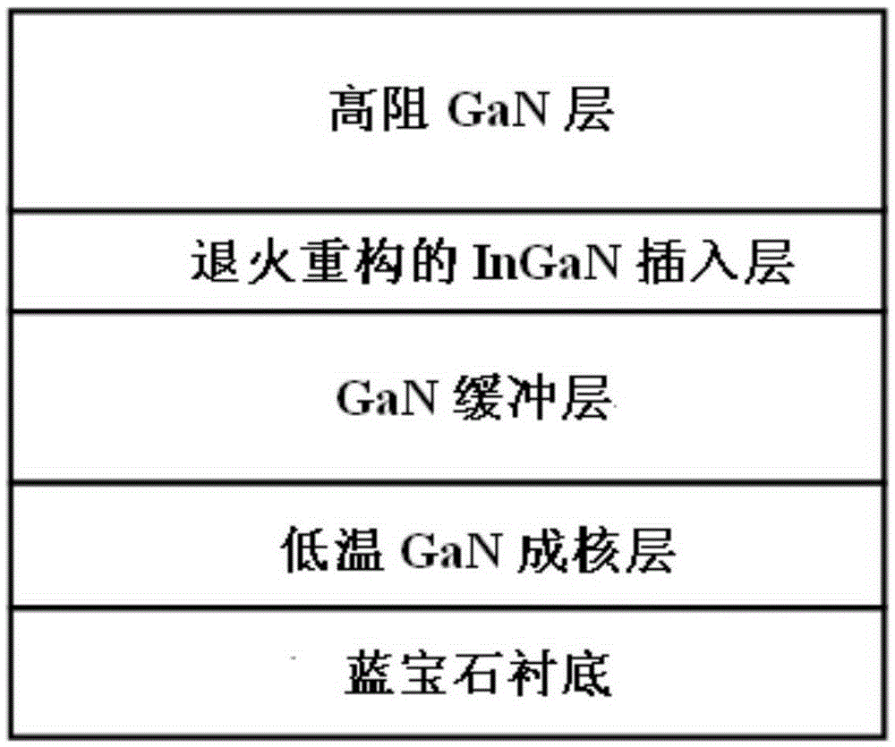
[0035] Such as figure 1 As shown, this embodiment provides an unintentionally doped high-resistance GaN film with an InGaN insertion layer, including:

[0036] - substrate, the material of which is sapphire;

[0037] - a low-temperature GaN nucleation layer, which is fabricated on the substrate, wherein the thickness of the low-temperature GaN nucleation layer is 25nm;

[0038] —GaN buffer layer, which is made on the low-temperature GaN nucleation layer, with a growth temperature of 1045°C and a thickness of 3.2 μm;

[0039] —Annealed and reconstructed InGaN insertion layer, which is fabricated on the GaN buffer layer, with a thickness of about 65nm; the growth temperature of the InGaN insertion layer is 770°C, and after the growth is completed, the temperature is raised to 1050°C for high-temperature annealing for 600s.

[0040] - A high-resistance GaN layer, which is fabricated on the annealed and reconstructed InGaN insertion layer, with a growth temperature of 1050° C. a...

Embodiment 2

[0052] This embodiment discloses an unintentionally doped high-resistance GaN film with an InGaN insertion layer. By introducing an InGaN insertion layer and annealing at a high temperature, an appropriate amount of edge dislocations, and a small amount of screw dislocations, using edge dislocations to induce carbon acceptors in the reaction chamber to incorporate into the GaN film, and then compensate the background electrons to achieve a high-resistance GaN film.

[0053] Specifically, the unintentionally doped high-resistance GaN thin film with an InGaN insertion layer includes: a sapphire layer, a low-temperature GaN nucleation layer, a GaN buffer layer, an annealed and reconstructed InGaN insertion layer, a high barrier GaN layer. The thickness of the low-temperature GaN nucleation layer is 30 nm, the thickness of the GaN buffer layer is 2 μm; the thickness of the annealed and reconstructed InGaN insertion layer is 100 nm, and the thickness of the high resistance GaN laye...

Embodiment 3

[0063] This embodiment discloses an unintentionally doped high-resistance GaN thin film with an InGaN insertion layer, including: an unintentional doped high-resistance GaN thin film with an InGaN insertion layer, including substrates arranged in sequence from bottom to top Bottom, low temperature GaN nucleation layer, GaN buffer layer, annealed and reconstructed InGaN insertion layer, high resistance GaN layer. The thickness of the low-temperature GaN nucleation layer is 30 nm; the thickness of the GaN buffer layer is 4 μm; the thickness of the annealed and reconstructed InGaN insertion layer is 90 nm; the thickness of the high resistance GaN layer is 1.5 μm.

[0064] The method for preparing an unintentionally doped high-resistance GaN film with an InGaN insertion layer in this embodiment includes the following steps:

[0065] Step 1: placing the substrate in a reaction chamber for heat treatment;

[0066] Step 2: using a two-step growth method to grow a low-temperature GaN...


PUM

PropertyMeasurementUnit
Thicknessaaaaaaaaaa
Thicknessaaaaaaaaaa
Layer thicknessaaaaaaaaaa

Abstract

The present invention provides an unintentionally doped high resistance GaN film with an InGaN insertion layer and a preparation method thereof. The unintentionally doped high resistance GaN film comprises a substrate, a low-temperature GaN nucleation layer, a GaN buffer layer, an InGaN insertion layer reconstructed by annealing and a high resistance GaN layer which are orderly arranged from bottom to top. Through introducing the InGaN insertion layer and carrying out high-temperature annealing, in the condition of not reducing GaN growth pressure and ensuring high crystal quality of the film, an appropriate amount of edge dislocations is introduced, a small amount of screw dislocations is increased, by using the edge dislocations, the carbon acceptor in a reaction chamber is induced into the GaN film, thus background electrons are compensated, and the high resistance GaN film is realized.

Description

technical field [0001] The invention relates to semiconductor material technology, in particular to an unintentionally doped high-resistance GaN film with an InGaN insertion layer and a preparation method thereof. Background technique [0002] At present, the third-generation wide bandgap semiconductor materials represented by GaN are widely used in the production of high frequency, high Electronic devices such as power and radiation resistance play a pivotal role. The high electron mobility transistor (HEMT) fabricated with AlGaN / GaN heterojunction has a high density and high mobility two-dimensional electron gas, which is an ideal material for the development of microwave power devices. At present, the most commonly used technology for preparing GaN material devices is metal-organic chemical vapor deposition (MOCVD) technology. However, GaN films grown by MOCVD contain a large number of donor defects such as O impurities and N vacancies, which will produce a high backgrou...

Claims


Application Information

Patent Timeline
IPC IPC(8): H01L29/06H01L29/20H01L21/02
CPCH01L29/0684H01L21/0242H01L21/02458H01L21/02502H01L21/0254H01L21/0262H01L29/2003
Inventor 梁红伟刘建勋柳阳夏晓川杜国同蒋建华闫晓密
Owner DALIAN UNIV OF TECH
Why Eureka
Try Eureka