
A three-dimensional microfluidic chip and its preparation method

A microfluidic chip and microfluidic technology, applied in chemical instruments and methods, laboratory containers, laboratory utensils, etc., can solve the problems of easy adsorption of organic solvents, difficulties in shaping and bonding, and easy blockage of microchannels and other problems, to achieve the effect of simple preparation method, increase the probability of successful preparation, and easy removal

Active Publication Date: 2017-08-25
WUHAN TEXTILE UNIV
View PDF1 Cites 0 Cited by
  • Summary
  • Abstract
  • Description
  • Claims
  • Application Information

AI Technical Summary

Problems solved by technology

Polymer materials can be used to prepare microfluidic channels by masking or 3D printing, and have a high degree of freedom in shaping. However, they are easy to deform and absorb organic solvents, and their analysis accuracy is far inferior to that of hard materials. chip
Although hard materials have stable performance and high analysis accuracy, shaping and bonding are relatively difficult
[0004] In the prior art, a relatively complex three-dimensional microfluidic structure can be produced by stacking double-layer hard substrates to match the microfluidic structures of the hard substrates. However, the bonding method of the hard substrates is currently There are only low-temperature bonding and gluing methods; among them, the low-temperature bonding method can only be used for glass chips, and has high requirements on the smoothness and cleanliness of the glass surface, requiring cumbersome cleaning steps; and the gluing method, as disclosed in the patent document CN103263950A A method for manufacturing a glass-based hybrid microfluidic chip is proposed, using double-sided adhesive to combine two layers of glass substrates, and the double-sided adhesive not only easily blocks the microchannel during the bonding process, but also requires a long curing time. In the process of use, the bond is not strong and easy to fall off

Method used


Image

  • A three-dimensional microfluidic chip and its preparation method
  • A three-dimensional microfluidic chip and its preparation method
  • A three-dimensional microfluidic chip and its preparation method

Examples


preparation example Construction

[0032] The preparation method of the microfluidic chip comprises the following steps:

[0033] (1) The prefabricated polymer (usually a mixture of polymer monomer and crosslinking agent, which can be cured at room temperature or heat to obtain a polymer) is evenly coated on a smooth substrate by spin coating or printing After curing at room temperature or heat, a polymer layer of 1 μm to 5 mm can be obtained; by controlling the preparation process, the thickness of the polymer layer can be controlled. For example, when the polymer layer is prepared by the spin coating method, spin at a speed of 1500r / min for 35 seconds A polymer layer of about 20 μm can be obtained, and the higher the rotation speed, the smaller the concentration of the prefabricated polymer, the longer the rotation time, the thinner the polymer layer, and when using the printing method, the thinner the hole network, the prepared The polymer layer is also thinner; and the choice of the substrate is related to ...

Embodiment 1

[0038] A microfluidic chip is composed of a first substrate and a second substrate, the surfaces of the first substrate and the second substrate are connected by a polymer layer of 5mm, the preparation method of the chip is as follows figure 1 Shown:

[0039] 1) Preparation of substrate chip:

[0040] Select two silicon wafers as the substrate, and process the required microfluidic structure on the silicon wafer, then rinse the chip with deionized water to remove impurities such as oil and particles on the surface of the substrate, clean it and put it in a clean working area Dry on a hot table for later use.

[0041] 2) Preparation of polymer:

[0042] The polymer described here is PDMS. Add the PDMS elastomer and PDMS curing agent into the paper cup at a ratio of 10:1, then use a clean glass rod to stir the mixture in one direction until there are uniform small bubbles in the mixture, then let the stirred mixture stand until the air bubbles are completely eliminated.

[00...

Embodiment 2

[0052] 1) Preparation of substrate chip:

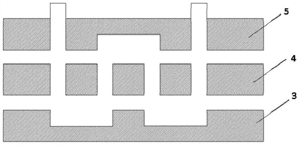
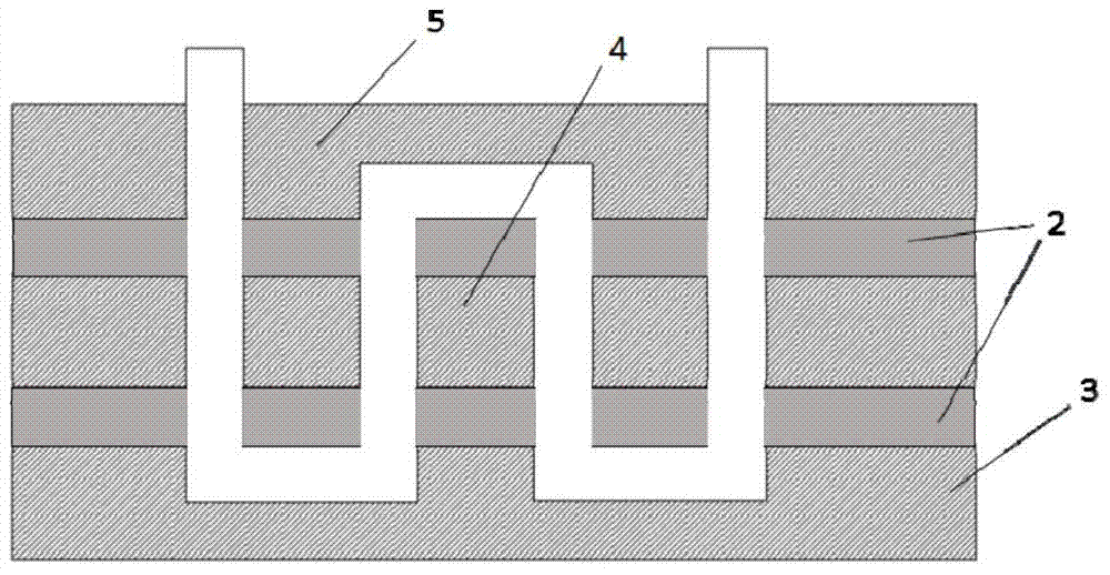
[0053] Select three glass chips as the first substrate, the second substrate and the third substrate respectively, and process the microfluidic structure respectively, such as Figure 2a As shown, there are first substrate 3 , second substrate 4 and third substrate 5 from bottom to top. Then rinse the chip with deionized water to remove impurities such as oil and particles on the surface of the substrate. After cleaning, put it on the hot table in the clean work area to dry for later use.

[0054] 2) Preparation of film:

[0055] The adhesive film described here is a PET adhesive film. Cut the adhesive film according to the principle that the adhesive film is larger than the base chip size, and then clean the adhesive film with deionized water until the color pattern is not visible to the light and does not hang water, and then put the cleaned film in the clean work area Dry on the hot table, the temperature of the hot table is 65 ...


PUM


Abstract

The invention discloses a three-dimensional microfluidic chip, comprising a first substrate, a second substrate, ... to an Nth substrate, N is a positive integer greater than or equal to 2, and the first substrate to the Nth substrate The sheet has a microfluidic channel or a microfluidic chamber, and the first substrate to the Nth substrate are connected in turn by two polymer layers, so that the microfluidic channel or microfluidic chamber of the first substrate to the Nth substrate are connected to form a three-dimensional microfluidic structure. The invention also discloses the preparation method of the microfluidic chip. First, the prefabricated polymer is uniformly coated on the substrate, and after drying, a polymer layer of 1 μm to 100 μm is obtained; then the first substrate and the second substrate are respectively It is bonded with the polymer layer and stacked repeatedly to obtain the microfluidic chip. Through the present invention, the bonding of the microfluidic chip can be realized without applying pressure, the method is simple, and can be widely used in the preparation of the microfluidic chip.

Description

technical field [0001] The invention belongs to the field of microfluidic chips, and more specifically relates to a three-dimensional microfluidic chip and a preparation method thereof. Background technique [0002] The microfluidic chip is the core of the micro-total analysis system. The invention and application of the microfluidic chip has provided great convenience to the scientific fields such as chemistry, food, environment, and medicine, and promoted the miniaturization, integration, automation and convenience of some analyzes change. It greatly saves the consumption of expensive chemical reagents for some chemical reactions, and also greatly improves the analysis efficiency and reduces the cost. [0003] The materials of microfluidic chips include polymers, such as PDMS (polydimethylsiloxane), PMMA (polymethyl methacrylate), etc., as well as hard materials, such as glass sheets, quartz sheets, etc. Polymer materials can be used to prepare microfluidic channels by m...

Claims


Application Information

Patent Timeline
Patent Type & Authority Patents(China)
IPC IPC(8): B01L3/00
Inventor 刘侃陈婷艾钊项坚真
Owner WUHAN TEXTILE UNIV
Learn More