Silicon-based and quantum dot fully integrated image sensor and preparation method

An image sensor and quantum dot technology, applied in the field of image sensors, can solve the problems of complex optical path and system design, high price, etc., and achieve the effect of saving chip area and reducing difficulty

Active Publication Date: 2016-03-16
SHANGHAI INTEGRATED CIRCUIT RES & DEV CENT +1
View PDF4 Cites 12 Cited by
  • Summary
  • Abstract
  • Description
  • Claims
  • Application Information

AI Technical Summary

Problems solved by technology

This technology product requires at least two image sensor chips for visible light and short-wave infrared, which makes the entire optical path and system design very c

Method used


Image

  • Silicon-based and quantum dot fully integrated image sensor and preparation method
  • Silicon-based and quantum dot fully integrated image sensor and preparation method
  • Silicon-based and quantum dot fully integrated image sensor and preparation method

Examples


Embodiment Construction

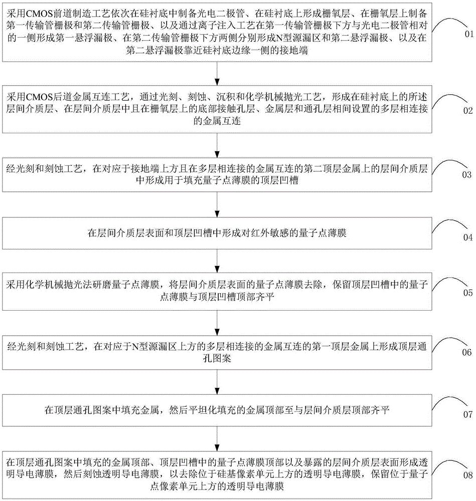
[0031] In order to make the content of the present invention clearer and easier to understand, the content of the present invention will be further described below in conjunction with the accompanying drawings. Of course, the present invention is not limited to this specific embodiment, and general replacements known to those skilled in the art are also covered within the protection scope of the present invention.

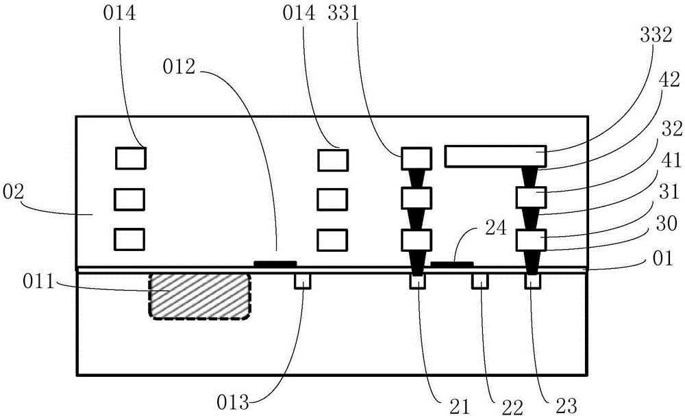
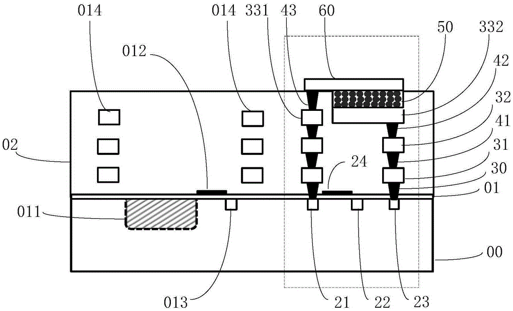
[0032] The absorption of incident light by a silicon-based CMOS image sensor depends on the junction depth of the photodiode. The longer the wavelength, the deeper the required junction depth. Photodiodes sensitive to visible light cannot sense infrared signals at the same time. If you need to be sensitive to infrared, you need to use larger injection energy to form a deeper photodiode. Larger injection energy will cause injection damage, increase dark current, and affect image quality, and the deeper the junction will be, the deeper the charge signal will be. The ...


PUM


Abstract

Disclosed are a silicon-based and quantum dot fully integrated image sensor and a preparation method. Silicon-based pixel units and quantum dot pixel units are integrated on a same silicon substrate, so the silicon-based image sensor can achieve imaging and detection for visible light; and an appropriate quantum dot material and an appropriate quantum dot size are selected, so an infrared high-sensitivity quantum dot thin film can be formed, imaging and detection for an infrared signal are achieved, and a photoelectric signal generated by the quantum dot thin film is controlled and read out on the basis that devices are formed on silicon bases. The quantum dot thin film pixel units and the silicon-based pixel units can achieve reuse of a readout circuit, the area of a chip is saved, and the difficulty of circuit design is reduced; the preparation method of the invention is compatible with CMOS image sensor process, the preparation method is in favor of single-chip manufacture of visible light and infrared image sensors, visible light and infrared detection technology combined wide spectrum detection and imaging technology is achieved, the complex degree of a product is simplified, and product cost is lowered.

Description

technical field [0001] The invention relates to the technical field of image sensors, in particular to an image sensor fully integrated with a silicon base and quantum dots and a preparation method thereof. Background technique [0002] An image sensor refers to a device that converts optical signals into electrical signals, which can be prepared based on charge-coupled device (CCD) technology, complementary metal-oxide-semiconductor (CMOS) image sensing technology, or quantum dot-based photodetection technology. [0003] CMOS image sensor refers to the image sensor technology processed on a silicon substrate using a CMOS process. Because of its low power consumption, low cost, mature technology, and compatibility with CMOS processes, it has been widely used in various fields. . CMOS image sensors are not only used in the field of consumer electronics, such as miniature digital cameras (DSC), mobile phone cameras, video cameras and digital single-lens reflex cameras (DSLR),...

Claims


Application Information

Patent Timeline
IPC IPC(8): H01L27/146
Inventor 赵宇航顾学强胡少坚
Owner SHANGHAI INTEGRATED CIRCUIT RES & DEV CENT
Why Eureka
Try Eureka