Single-crystal film bonding body and manufacturing method thereof

A technology of single crystal thin film and bonding body, which is applied in semiconductor/solid-state device manufacturing, crystal growth, single crystal growth, etc. It can solve the problems of unfavorable direct bonding at the bonding interface and failure of direct bonding, etc., and achieve the elimination of directional reflection , eliminate interference, eliminate the effect of reflection

Inactive Publication Date: 2016-03-23
JINAN JINGZHENG ELECTRONICS
View PDF4 Cites 27 Cited by
  • Summary
  • Abstract
  • Description
  • Claims
  • Application Information

AI Technical Summary

Problems solved by technology

However, the rough bonding interface is very unfavorable for direct bonding, and even the direct bonding cannot be successful

Method used


Image

  • Single-crystal film bonding body and manufacturing method thereof
  • Single-crystal film bonding body and manufacturing method thereof
  • Single-crystal film bonding body and manufacturing method thereof

Examples


example 1

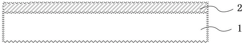
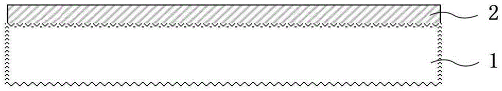
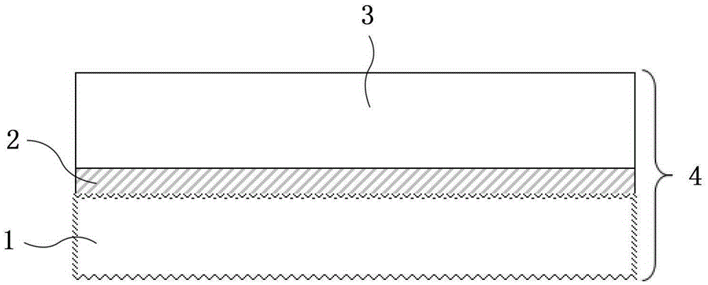
[0063] The original substrate is a lithium niobate wafer with a thickness of 200 microns and a surface roughness of micron or submicron level, such as 0.1 micron to 2 microns, which can be roughened by grinding, etching or sandblasting. Deposit a layer of silicon thin film as a transition layer on the rough surface of lithium niobate by sputtering process, the film thickness is 2 microns; anneal the deposited sheet after deposition, the annealing temperature is 300°C, and the annealing time is 5 hours. The surface of the silicon transition layer on the deposition sheet is chemically mechanically polished to make the surface roughness of the silicon transition layer less than 1 nanometer; the target substrate is a silicon substrate with a thickness of 500 microns, and the silicon substrate is chemically mechanically polished to make the surface roughness less than 1 nm. After the original substrate and the target substrate are cleaned, the polished surface of the silicon transi...

example 2

[0065] The original substrate was a lithium tantalate wafer with a thickness of 350 microns and a surface roughness of 0.2 microns. Deposit a layer of silicon film as a transition layer by evaporation process, with a thickness of 1.5 microns; anneal the deposited sheet after deposition at 200°C for 3 hours to remove defects and impurities in the silicon film. The surface of the silicon transition layer is chemically mechanically polished to make the surface roughness lower than 1 nanometer; the target substrate is a silicon substrate with a thickness of 650 microns, and the silicon substrate is chemically mechanically polished to make the surface roughness lower than 1 nanometer. After the original substrate and the target substrate are cleaned, the polished surface of the silicon transition layer and the polished surface of the silicon substrate are bonded by using a direct bonding process to form a bonded body. The bonding body is annealed at 170° C. for 2 hours to further e...

example 3

[0067] The original substrate is a lithium tantalate wafer with a thickness of 250 microns and a surface roughness of micron or submicron level. Deposit a layer of silicon dioxide as a transition layer by plasma-enhanced chemical vapor deposition process, the deposition thickness is 3 microns, the deposition temperature is 200°C, and the silicon dioxide deposition sheet is annealed, the annealing temperature is 300°C, and the annealing time is 3 hours , to remove defects and impurities in the transition layer. The silicon dioxide surface is chemically mechanically polished to make the surface roughness lower than 1 nanometer; the target substrate is a silicon substrate with a thickness of 500 microns, and the silicon substrate is chemically mechanically polished to make the surface roughness lower than 1 nanometer. After cleaning the original substrate and the target substrate, a direct bonding process is used to bond the polished surface of the silicon dioxide transition laye...


PUM

PropertyMeasurementUnit
thicknessaaaaaaaaaa
thicknessaaaaaaaaaa
thicknessaaaaaaaaaa

Abstract

The invention provides a single-crystal film bonding body and a method for manufacturing the single-crystal film bonding body. The single-crystal film bonding body comprises a silicon substrate, a lithium niobate single-crystal film or lithium tantalate single-crystal film and a silicon-based film located between the silicon substrate and the lithium niobate single-crystal film or lithium tantalate single-crystal film. The silicon-based film is formed on the lithium niobate single-crystal film or lithium tantalate single-crystal film through deposition and is bonded with the silicon substrate through a direct bonding method, and the silicon-based film is a silicon film or a silicon dioxide film or a silicon nitride film. By means of the single-crystal film bonding body of the three-layer structure, the reflection effect of interfaces between the lithium niobate or lithium tantalate single-crystal film and the silicon substrate on optical waves and sound waves can be effectively reduced and even eliminated, and the interference caused by the reflection effect between the interfaces to optical or sound wave signals is reduced.

Description

technical field [0001] The present invention relates to a single crystal thin film bonded body with a low interface reflectivity having a three-layer structure and a method for manufacturing the single crystal thin film bonded body, more particularly, to a substrate material capable of reducing light waves or sound waves The invention discloses a single crystal thin film bonded body whose interface is reflected and a method for manufacturing the single crystal thin film bonded body. Background technique [0002] Lithium tantalate single crystal thin film and lithium niobate thin film single crystal thin film have a wide range of applications in optical signal processing, information storage, and electronic devices. Using them as basic materials can make high-frequency, high-bandwidth, high-integration, large-scale capacity, low power optoelectronic devices and integrated optical circuits. In addition, lithium tantalate single crystal thin films and lithium niobate single cr...

Claims


Application Information

Patent Timeline
Patent Type & Authority Applications(China)
IPC IPC(8): C23C14/22C23C16/513C30B23/02C30B25/02H01L21/304
CPCC23C14/22C23C16/513C30B23/02C30B25/02H01L21/304H01L21/30625
Inventor 胡文
Owner JINAN JINGZHENG ELECTRONICS
Why Eureka
Try Eureka