Semiconductor light emitting element

A technology of light-emitting components and semiconductors, applied in semiconductor devices, electrical components, circuits, etc., can solve problems such as asymmetric distribution of electrons and holes, and achieve the effects of improving luminous efficiency, avoiding lattice quality, and increasing luminous intensity.

Active Publication Date: 2016-03-23
ANHUI SANAN OPTOELECTRONICS CO LTD
View PDF4 Cites 5 Cited by
  • Summary
  • Abstract
  • Description
  • Claims
  • Application Information

AI Technical Summary

Problems solved by technology

[0004] Aiming at the asymmetric distribution of electrons and holes in the traditional quantum well design, the present invention proposes a semiconductor light-emitting element with a composite structure to improve the recombination efficiency of electrons and holes and the light output area

Method used


Image

  • Semiconductor light emitting element
  • Semiconductor light emitting element
  • Semiconductor light emitting element

Examples


Embodiment 1

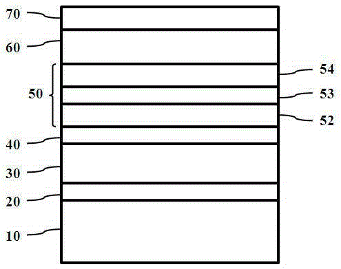
[0032] See attached figure 1 , a semiconductor element with a composite structure layer 50, comprising a substrate 10, and a nitride buffer layer 20, an n-type layer 30, a shallow quantum well layer 40, a multi-quantum well layer 60 and a p-type layer sequentially formed on the substrate 10 layer 70, and a composite structure layer 50 located between the shallow quantum well layer 40 and the multiple quantum well layer 60, wherein the substrate 10 is a sapphire flat substrate, a sapphire patterned substrate, a silicon nitride substrate, a GaN substrate , silicon substrate, glass substrate or metal substrate, the nitride buffer layer 20 is a single-layer structure or a superlattice structure, which is a binary or ternary structure composed of Ga, N, In, Al Or a quaternary structure; the p-type layer 70 is a Mg-doped GaN layer.

[0033] Continue to see attached figure 1 , in this embodiment, the composite structure layer 50 at least includes a p-type doped GaN layer 54, an n-t...

Embodiment 2

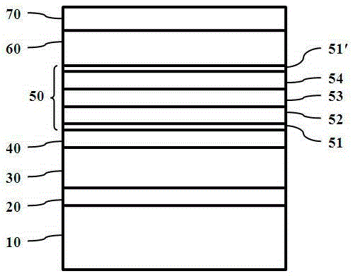
[0036] See attached figure 2 The difference between this embodiment and Embodiment 1 is that the composite structure layer 50 also includes a first electron blocking layer 51 adjacent to the shallow quantum well layer 40 and a second electron blocking layer 51' adjacent to the multi-quantum well layer 60, wherein, The materials of the first electron blocking layer 51 and the second electron blocking layer 51' are both AlGaN, and their thicknesses are the same or different. In this embodiment, the thicknesses of the electron blocking layer 51 and the second electron blocking layer 51' are preferably the same, and the preferred thickness range is Both are 400 angstroms to 600 angstroms.

[0037] Specifically, see the attached image 3 , the composite structure layer 50 from bottom to top is the first electron blocking layer 51, n-type doped GaN layer 52, Al x In y Ga 1-x-y N isolation layer 53, p-type doped GaN layer 54, and second electron blocking layer 51'; wherein, the ba...

Embodiment 3

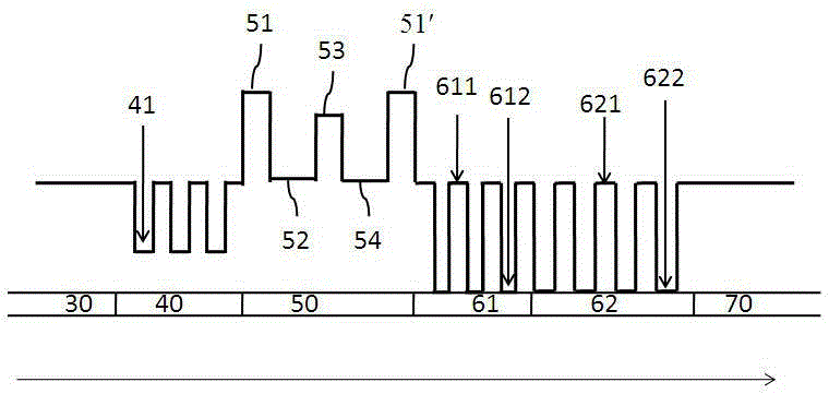
[0042] See attached Figure 4 The difference between this embodiment and Embodiment 1 is that the composite structure layer 50 at least includes a p-type doped GaN layer 54, an n-type doped GaN layer 52, and a layer between the p-type doped GaN layer 54 and the n-type doped GaN layer. The material between layers 52 is Al x In y Ga 1-x-y A periodic structure 50' composed of N isolation layers 53 alternately, a first electron blocking layer 51 adjacent to the shallow quantum well layer 40, and a second electron blocking layer 51' adjacent to the multi-quantum well layer 60, wherein the period of the periodic structure 50' The number is greater than or equal to 2, and each cycle includes n-type doped GaN layer 52, isolation layer 53, p-type doped GaN layer 54 and isolation layer 53, and the first electron blocking layer 51 and the second electron blocking layer 51' are rich in While collecting electrons in the composite structure layer 50, control the migration of the p-type i...


PUM


Abstract

The invention belongs to the technical field of semiconductors, and particularly relates to a semiconductor light emitting element. The semiconductor light emitting element comprises a substrate, and a nitride buffer layer, an n-type layer, a shallow quantum well layer, a multiple quantum well layer and a p-type layer formed on the substrate sequentially. The semiconductor light emitting element is characterized in that a composite structure layer is also inserted between the shallow quantum well layer and the multiple quantum well layer; the composite structure layer at least comprises a p-type doped GaN layer, an n-type doped GaN layer, and an isolation layer located between the p-type doped GaN layer and the n-type doped GaN layer. The feature that p-type impurities in the composite structure layer are migrated to the shallow quantum well layer and the multiple quantum well layer is used, light emitting of the shallow quantum well layer and the composite structure layer is promoted while the light-emitting strength of the multiple quantum well layer is enhanced, the light outgoing area of the semiconductor element is increased, and the light-emitting strength is further enhanced.

Description

technical field [0001] The invention belongs to the technical field of semiconductors, in particular to a semiconductor element with a composite structure layer. Background technique [0002] Light-emitting diodes (LED for short) have been widely used in the two fields of lighting and display due to their advantages of high efficiency, long life, all-solid-state, self-illumination and green environmental protection, especially the current development of white light lighting, making The market demand for LED epitaxial wafers and chips has increased sharply. [0003] At present, in the light-emitting diode structure, due to the low activation efficiency of p-type impurities, the concentration of activated holes in the p-type layer is much lower than the electron concentration in the n-type layer, and due to the small mobility of the holes, it is 480 cm 2 / Vs (only 1 / 3~1 / 2 of the electron mobility), so that the activated holes are mainly concentrated in the quantum well near t...

Claims


Application Information

Patent Timeline
Patent Type & Authority Applications(China)
IPC IPC(8): H01L33/06H01L33/14H01L33/00
CPCH01L33/06H01L33/145
Inventor 江汉蓝永凌黄文宾林兓兓张家宏
Owner ANHUI SANAN OPTOELECTRONICS CO LTD
Why Eureka
Try Eureka