Cheap disorder broad-spectrum wide-angle antireflection structure and manufacturing method thereof

A production method and wide-spectrum technology, applied in the direction of final product manufacturing, sustainable manufacturing/processing, electrical components, etc., can solve the problems of easy to improve battery cost performance, high price, high preparation process, etc., to improve photoelectric conversion efficiency and Other properties, the effect of simple preparation scheme and compatible preparation process

Inactive Publication Date: 2016-04-06
SUZHOU INST OF NANO TECH & NANO BIONICS CHINESE ACEDEMY OF SCI
View PDF6 Cites 6 Cited by
  • Summary
  • Abstract
  • Description
  • Claims
  • Application Information

AI Technical Summary

Problems solved by technology

[0003] As far as the field of photovoltaics is concerned, III-V solar cells and Si-based solar cells are the main components in the field of photovoltaics, but their high refractive index makes their reflection loss as high as 30% or more. However, the resulting surface non-radiative recombination makes it difficult to collect carriers and cannot effectively improve the efficiency of the cell. How to improve its wide-spectrum anti-reflection performance without destroying its surface carrier collection ability has always been a difficult problem in the field of photovoltaics.
[0004] Although coating the surface of solar cells with a dielectric film has

Method used


Image

  • Cheap disorder broad-spectrum wide-angle antireflection structure and manufacturing method thereof
  • Cheap disorder broad-spectrum wide-angle antireflection structure and manufacturing method thereof
  • Cheap disorder broad-spectrum wide-angle antireflection structure and manufacturing method thereof

Examples


Embodiment 1

[0047] 1. Deposit a dielectric film on the surface of the substrate material

[0048] SiO with a thickness of 520nm is deposited on the Si substrate by PECVD to form a dielectric film.

[0049] 2. Preparation of metal colloid solution (3.75%Ag)

[0050] The metal-organic colloid solution was prepared at a dilution ratio of 70% Agink: ethanol = 1:18.

[0051] 3. Preparation of metal colloid film

[0052] A metal film layer with a thickness of 140 nm was obtained on the dielectric film by a spin coating method.

[0053] 4. Preparation of metal nanostructures

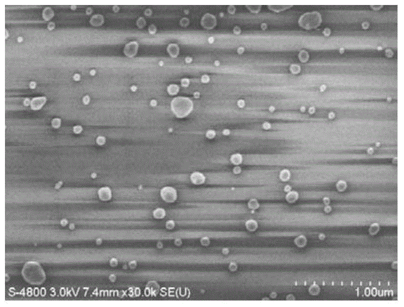
[0054] Metal nanostructures were obtained by heating at 280°C for 5 minutes by means of hot plate heating. figure 1 shown.

[0055] 5. Fabrication of anti-reflection structure

[0056] Using reactive ion etching, using SF 6 / CHF 3 / He three etching gases were etched for 2.5 minutes, and the etching depth was about 490 nm, and an anti-reflection structure with a disordered wide spectrum and wide angle was obtained. ...

Embodiment 2

[0059] 1. Deposit a dielectric film on the surface of the substrate material

[0060] SiO with a thickness of 520nm is deposited on the Si substrate by PECVD to form a dielectric film.

[0061] 2. Preparation of metal colloid solution (7.00%Ag)

[0062] The metal colloid solution was prepared at a dilution ratio of 70% Agink: ethanol = 1:9.

[0063] 3. Preparation of metal colloid film

[0064] A 220nm metal film layer was obtained on the dielectric film by a spin coating method.

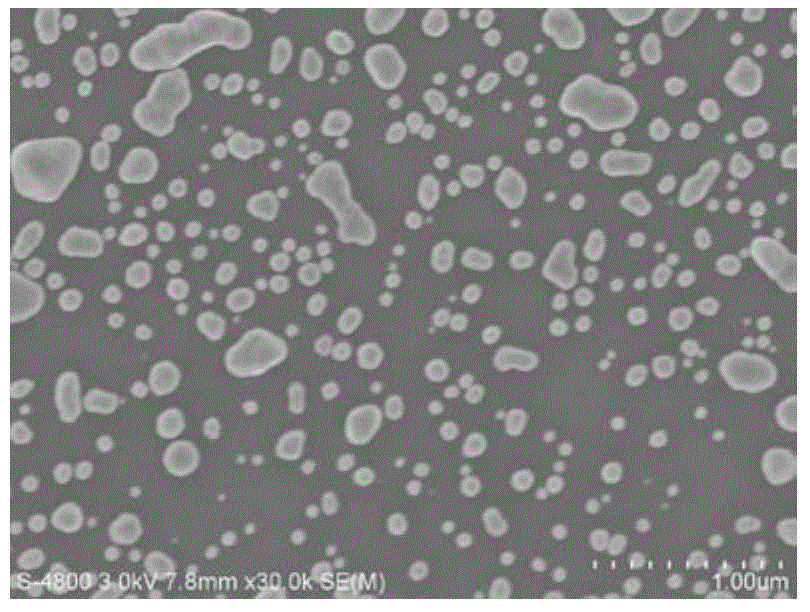
[0065] 4. Preparation of metal nanostructures

[0066] Metal nanostructures were obtained by heating at 350°C for 2 minutes by means of hot plate heating. figure 2 shown.

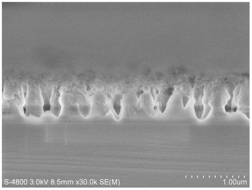
[0067] 5. Fabrication of anti-reflection structure

[0068] Using reactive ion etching, using SF 6 / CHF 3 / He three etching gases etch for 2.5min, and the etching depth is about 490nm, and the anti-reflection structure with disordered wide spectrum and wide angle is obtained. image 3 shown.

[0069] The metal nanostru...

Embodiment 3

[0071] 1. Deposit a dielectric film on the surface of the substrate material

[0072] SiO with a thickness of 520nm is deposited on the Si substrate by PECVD to form a dielectric film.

[0073] 2. Preparation of metal colloid solution (8.75%Ag)

[0074] The metal colloid solution was prepared with a dilution ratio of 70% Agink: ethanol = 1:7.

[0075] 3. Preparation of metal colloid film

[0076] A 260nm metal film layer was obtained on the dielectric film by a spin coating method.

[0077] 4. Preparation of metal nanostructures

[0078] Metal nanostructures were obtained by heating at 200°C for 10 minutes by means of hot plate heating. Figure 4 shown.

[0079] 5. Fabrication of anti-reflection structure

[0080] Using reactive ion etching, using SF 6 / CHF 3 / He three etching gases were etched for 2.5 minutes, and the etching depth was about 490 nm, and an anti-reflection structure with a disordered wide spectrum and wide angle was obtained.

[0081] The metal nanost...


PUM

PropertyMeasurementUnit
Thicknessaaaaaaaaaa

Abstract

The invention discloses a cheap disorder broad-spectrum wide-angle antireflection structure and a manufacturing method thereof. The manufacturing method comprises the steps of: s1, depositing a dielectric film on the surface of a substrate material (or structure); s2, forming a metal colloid film on the surface of the dielectric film; s3, heating the metal colloid film to obtain a metal nano structure; s4, etching the dielectric film by taking the metal nano structure as a mask to form the antireflection structure; s5, and removing the metal nano structure. The dielectric nano structure manufacturing scheme provided by the invention is simple and practicable, can achieve large-area manufacturing, only needs low temperature, and is low in manufacturing energy consumption and high in efficiency. In addition, the manufactured disorder dielectric nano structure and the residual metal mask can obtain excellent broad-spectrum wide-angle antireflection effect.

Description

technical field [0001] The application belongs to the field of optics and optoelectronics, in particular to a low-cost disordered wide-spectrum wide-angle anti-reflection structure and a manufacturing method thereof. Background technique [0002] Wide-spectrum and wide-angle anti-reflection is a functional characteristic of devices required in many optical fields. How to obtain the required wide-spectrum and wide-angle anti-reflection without compromising other functional characteristics of devices has always been the goal pursued by the fields of optics and optoelectronics. [0003] As far as the field of photovoltaics is concerned, III-V solar cells and Si-based solar cells are the main components in the field of photovoltaics, but their high refractive index makes their reflection loss as high as 30% or more. However, the resulting surface non-radiative recombination makes it difficult to collect carriers and cannot effectively improve cell efficiency. How to improve its ...

Claims


Application Information

Patent Timeline
IPC IPC(8): H01L31/18H01L31/0216
CPCY02P70/50
Inventor 张瑞英王岩岩
Owner SUZHOU INST OF NANO TECH & NANO BIONICS CHINESE ACEDEMY OF SCI
Why Eureka
Try Eureka