Metal patterning method

A metal pattern and pattern structure technology, applied in metal material coating process, gaseous chemical plating, decorative arts, etc., can solve the problem of destroying the direct contact between the metal and the imprinted sample, increasing the edge roughness of the imprinting pattern, and affecting the pattern. Accuracy and other issues, to achieve the effect of reducing edge roughness, improving processing efficiency and high precision

Active Publication Date: 2016-04-20
SUZHOU INST OF NANO TECH & NANO BIONICS CHINESE ACEDEMY OF SCI
View PDF7 Cites 4 Cited by
  • Summary
  • Abstract
  • Description
  • Claims
  • Application Information

AI Technical Summary

Problems solved by technology

However, the micro-contact pattern transfer technology in the prior art mostly uses a single layer of organic chemical molecules to coat the imprinted sample to improve the adhesion of the metal film or a single layer of organic chemical molecules to coat the metal film on the embossed plate to form a pattern. etch mask, but this will destroy the direct contact between the metal and the imprinted sample, increasing the contact resistance, and the latter also has the problem of surface diffusion of the monolayer of organic chemical molecules, which affects the accuracy of the pattern
In addition, the graphics on the embossed plates used in these technologies have a positive mesa structure, which is suitable for the transfer of three-dimensional graphics, but greatly increases the edge roughness of the imprinted graphics

Method used


Image

  • Metal patterning method
  • Metal patterning method
  • Metal patterning method

Examples


Embodiment 1

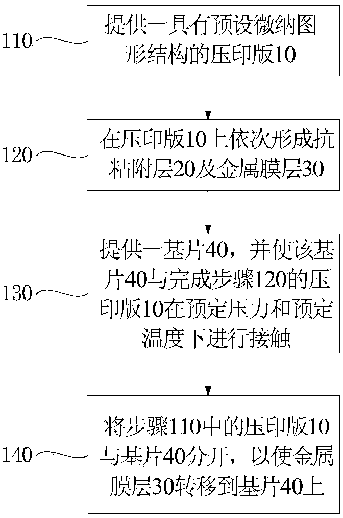
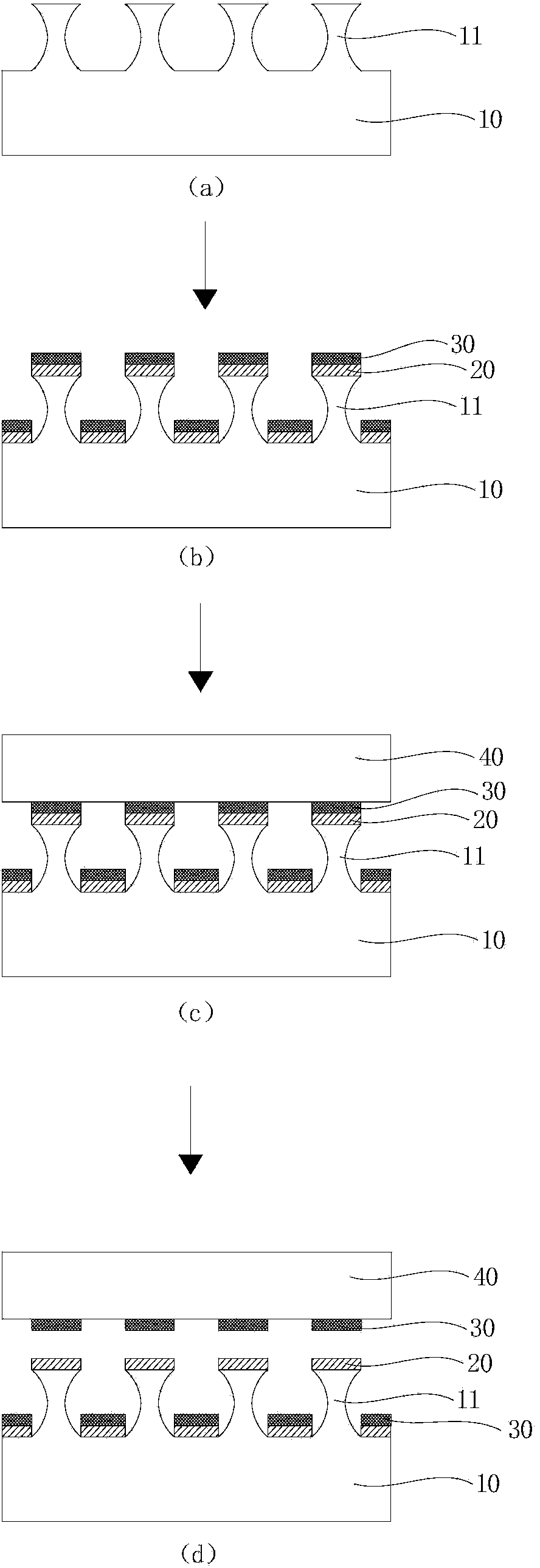
[0042] based on figure 1 and figure 2 The process flow diagram shown provides a silicon imprint plate with a preset micro-nano pattern structure and a substrate formed of polyethylene terephthalate (PET). First, using octafluorocyclobutane (C 4 f 8 ) gas at 300 watts power and 20 millitorr pressure to deposit an anti-adhesion layer formed by fluorocarbons on the silicon imprint plate; secondly, deposit a thickness of 100 nanometers on the anti-adhesion layer by electron beam evaporation process The gold film layer; then, use an optical microscope to align the silicon imprint plate with the substrate, and apply 5 standard atmospheric pressure to make the two compact, and raise the temperature to 100 degrees Celsius and keep it for 3 minutes; finally, naturally cool to room temperature And the pressure is removed to separate the silicon imprint plate from the substrate, thereby forming a nanometer metal structure (or called a metal pattern) on the substrate.

[0043] Figu...

Embodiment 2

[0048] based on figure 1 and figure 2 As shown in the process flow chart, a quartz imprint plate with a predetermined micro-nano pattern structure and a substrate formed of polyethylene terephthalate (PET) are provided. First, using octafluorocyclobutane (C 4 f 8 ) gas at 300 watts power and 20 millitorr pressure to deposit an anti-adhesion layer formed by fluorocarbons on the quartz imprint plate; secondly, deposit a thickness of 100 nanometers on the anti-adhesion layer by using electron beam evaporation process The aluminum film layer; then, use an optical microscope to align the quartz imprint plate with the substrate, and apply 10 standard atmospheres to make the two compact, and raise the temperature to 110 degrees Celsius and keep it for 3 minutes; finally, naturally cool to 40 Celsius and the pressure is removed to separate the quartz imprint plate from the substrate, thereby forming a nano-metal structure (or metal pattern) on the substrate.

[0049] Figure 7 I...

Embodiment 3

[0052] based on figure 1 and figure 2 The process flow diagram shown provides a silicon imprint plate with a predetermined micro-nano pattern structure (such as a one-dimensional grating pattern structure) and a substrate formed of polyethylene terephthalate (PET). First, using octafluorocyclobutane (C 4 f 8 ) gas at 300 watts power and 20 millitorr pressure to deposit an anti-adhesion layer formed by fluorocarbons on the silicon imprint plate; secondly, deposit a thickness of 100 nanometers on the anti-adhesion layer by electron beam evaporation process The aluminum film layer; then, use an optical microscope to align the silicon imprint plate with the substrate, and apply 10 standard atmospheric pressure to make the two compact, and raise the temperature to 110 degrees Celsius and keep it for 3 minutes; finally, naturally cool to 40 Celsius and the pressure is removed to separate the silicon imprint plate from the substrate, thereby forming a nano-metal structure on the ...


PUM


Abstract

The invention discloses a metal patterning method. The metal patterning method comprises the following steps: A) providing an imprinting plate with a preset micro-nano pattern structure; B) forming an anti-adhesion layer and a metal film layer in sequence on the imprinting plate; C) providing a substrate, and making the substrate come into contact with the imprinting plate being subjected to the step B) under a predetermined pressure and at a predetermined temperature; and D) separating the imprinting plate obtained in the step A) from the substrate to transfer the metal film layer onto the substrate in order to form a nano-metal structure on the substrate. According to the metal patterning method disclosed by the invention, the imprinting plate provided with a structural body of which a side wall is indent is utilized, so that the edge roughness of the nano-metal structure transferred onto the substrate can be reduced effectively, and metal patterning in a vacuum environment can be realized. Moreover, the metal patterning method is high in accuracy and simple in process; the cost of metal patterning, particularly metal nano-structure patterning is lowered greatly; and meanwhile the machining efficiency can be increased.

Description

technical field [0001] The invention belongs to the technical field of micro-nano processing, and in particular relates to a metal patterning method. Background technique [0002] Patterning is one of the most important technologies in the field of micro-nano processing technology. Among them, metal patterning is extremely important for preparing electrodes, realizing optical interconnection and forming etching masks. The metal patterning technology in the prior art generally adopts the technology of optical exposure and development to define the pattern, and forms the pattern by etching. This technique uses a lot of organic reagents, which is difficult to apply to organic electronic devices. In addition, this liquid-phase process technology cannot meet the demand for patterning technology in a vacuum environment. Considering the high-efficiency preparation of nanostructures, common optical exposure techniques are also limited by precision. [0003] Microcontact pattern t...

Claims


Application Information

Patent Timeline
Patent Type & Authority Applications(China)
IPC IPC(8): B81C1/00
Inventor 陈沁
Owner SUZHOU INST OF NANO TECH & NANO BIONICS CHINESE ACEDEMY OF SCI
Why Eureka
Try Eureka