A kind of diamond/copper gradient composite material and its preparation method
A composite material and diamond technology, applied in the field of diamond/copper gradient composite material and its preparation, can solve the problems of bulging, complex process, reduced surface roughness, etc., to meet the needs of chip connection, the process is simple, and the roughness is reduced. Effect
- Summary
- Abstract
- Description
- Claims
- Application Information
AI Technical Summary
Problems solved by technology
Method used
Image
Examples
Embodiment 1
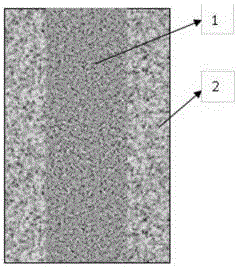
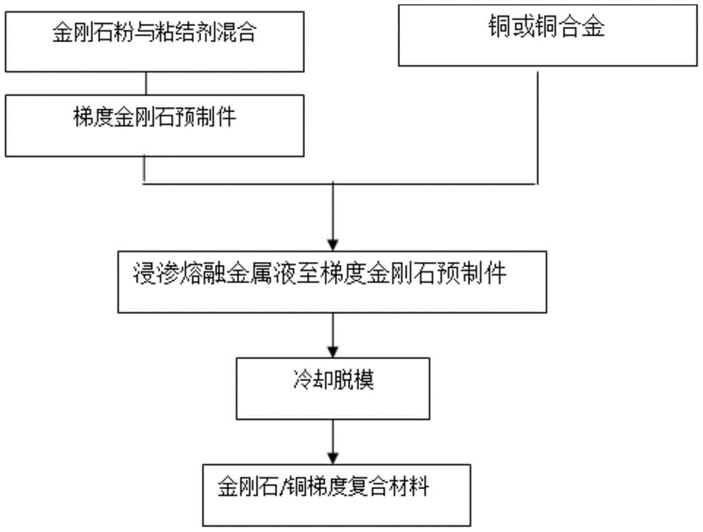
[0022] according to figure 1 In the process shown, the coarse-grained diamond used is 250 μm, the fine-grained diamond is 60 μm, the binder is paraffin-based binder, the thickness of the coarse-grained diamond layer is 2 mm, and the thickness of the fine-grained diamond layers on both sides is 0.5 mm. , cold pressing pressure 50MPa, holding pressure for 3min, demoulding, drying at 95°C for 2h to obtain gradient diamond preforms, diamond / copper gradient composite materials prepared after impregnating copper, figure 1 Its structural diagram, in which 1 is a coarse-grained diamond / copper composite layer, and 2 is a fine-grained diamond / copper composite layer, with distinct layers; its thermal conductivity reaches 638W / mK, and the surface roughness Ra after processing into products is 0.4-0.5 μm.
Embodiment 2
[0024] according to figure 1 In the process shown, the coarse-grained diamond is 100 μm, the fine-grained diamond is 60 μm, and the binder is phosphate binder. The thickness of the coarse-grained diamond layer is 2 mm, and the thickness of the fine-grained diamond layers on both sides is 0.5 mm. , cold pressing pressure 60MPa, holding pressure for 3min, demoulding, drying at 110°C for 2.5h to obtain a gradient diamond preform, and the diamond / copper gradient composite material prepared after impregnating copper, with a thermal conductivity of 550W / mK, processing The finished product has a surface roughness Ra of 0.4-0.5 μm.
Embodiment 3
[0026] according to figure 1 In the process shown, the coarse-grained diamond used is 120 μm, the fine-grained diamond is 40 μm, the binder is paraffin-based binder, the thickness of the coarse-grained diamond layer is 1 mm, and the thickness of the fine-grained diamond layers on both sides is 1 mm. Cold pressing pressure 70MPa, holding pressure for 3min, demoulding, drying at 100°C for 2h to obtain gradient diamond preform, diamond / copper gradient composite material prepared after infiltration of copper alloy, thermal conductivity reaches 500W / mK, processed into The surface roughness Ra after the product is 0.3-0.4 μm.
PUM
| Property | Measurement | Unit |
|---|---|---|
| size | aaaaa | aaaaa |
| size | aaaaa | aaaaa |
| thickness | aaaaa | aaaaa |
Abstract
Description
Claims
Application Information

