Preparation method of epitaxial wafer for FRD

A silicon epitaxial wafer and epitaxial layer technology, which is used in semiconductor/solid-state device manufacturing, electrical components, circuits, etc., can solve the problems of unstable device parameters, short transition zone, resistance to reverse recovery current impact, etc., to improve softness factor, good consistency, the effect of maintaining electrical characteristics

Inactive Publication Date: 2016-05-11
HEBEI POSHING ELECTRONICS TECH
View PDF6 Cites 6 Cited by
  • Summary
  • Abstract
  • Description
  • Claims
  • Application Information

AI Technical Summary

Problems solved by technology

[0009] The conventional epitaxial process is to grow the epitaxial layer directly on the substrate by the method of constant injection and dilution flow, and the concentration of the epitaxial layer is constant. The transition zone formed by this method is very short, and the ability to resist the impact of reverse recovery current is very small.
The traditional manufacturing method of buffer layer is to use implantation and diffusion process to form buffer layer and N+ layer on the N- substrate. Due to the uncontrollable implantation process, parameters such as impurity concentration, buffer layer thickness, and impurity concentration distribution of the buffer layer are uncontrollable. , eventually leading to the instability of device parameters

Method used


Image

  • Preparation method of epitaxial wafer for FRD
  • Preparation method of epitaxial wafer for FRD
  • Preparation method of epitaxial wafer for FRD

Examples


Embodiment Construction

[0029] The technical solutions in the embodiments of the present invention are clearly and completely described below in conjunction with the accompanying drawings in the embodiments of the present invention. Obviously, the described embodiments are only part of the embodiments of the present invention, not all of them. Based on the embodiments of the present invention, all other embodiments obtained by persons of ordinary skill in the art without making creative efforts belong to the protection scope of the present invention.

[0030] In the following description, a lot of specific details are set forth in order to fully understand the present invention, but the present invention can also be implemented in other ways different from those described here, and those skilled in the art can do it without departing from the meaning of the present invention. By analogy, the present invention is therefore not limited to the specific examples disclosed below.

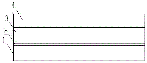
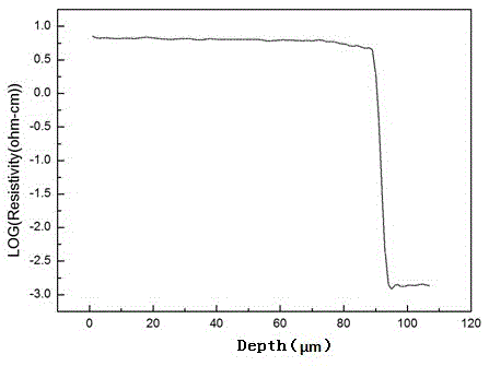
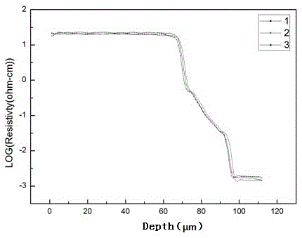
[0031] The invention di...


PUM

PropertyMeasurementUnit
electrical resistivityaaaaaaaaaa
thicknessaaaaaaaaaa
electrical resistivityaaaaaaaaaa

Abstract

The invention discloses a preparation method of an epitaxial wafer for FRD, relating to the technical field of a method of depositing a semiconductor material on a substrate. The method comprises the following steps: growing an intrinsic layer on the upper surface of a silicon substrate; fixing the flow of a silicon source, reducing the flow of an injected dopant gradually and increasing the flow of diluted hydrogen gradually at the same time, so as to grow a buffer layer with gradually varying impurity concentration on the upper surface of the intrinsic layer; and growing an epitaxial layer on the buffer layer. According to the method, through controlling the flow, a controllable long-transition-area epitaxial layer with gradually varying epitaxial concentration is formed; therefore, the soft factor of a device can be improved and the original electric property of the device can be maintained.

Description

technical field [0001] The invention relates to the technical field of deposition methods of semiconductor materials on substrates, in particular to a method for preparing silicon epitaxial wafers for FRD. Background technique [0002] Under the forward bias voltage, the conduction resistance of the PIN structure diode is very small, which is close to a short circuit; under the reverse bias voltage, the impedance is very high, close to an open circuit; and it has the characteristics of large power capacity, small loss, fast speed, etc., so in Widely used in power diodes. For example: In electronic circuits such as switching power supplies, PWM pulse width modulators, and frequency converters, they are used as high-frequency rectifier diodes, freewheeling diodes, or damping diodes. [0003] With the continuous development of electronic technology and integrated circuits, higher requirements are put forward for the stability and reliability of power semiconductor devices. Fo...

Claims


Application Information

Patent Timeline
Patent Type & Authority Applications(China)
IPC IPC(8): H01L21/02
CPCH01L21/02381H01L21/0245H01L21/0251H01L21/02532H01L21/0257H01L21/02634
Inventor 吴会旺
Owner HEBEI POSHING ELECTRONICS TECH
Why Eureka
Try Eureka