
A kind of thin film transistor based on zinc oxide thin film

A thin film transistor, zinc oxide thin film technology, applied in transistors, semiconductor devices, electrical components, etc., can solve problems such as the stability of zinc oxide thin film transistors, device performance degradation, high carrier concentration, etc. The effect of reducing interface defect density, improving internal crystalline structure, and high mobility

Active Publication Date: 2019-01-15
ZHEJIANG UNIV
View PDF3 Cites 0 Cited by
  • Summary
  • Abstract
  • Description
  • Claims
  • Application Information

AI Technical Summary

Problems solved by technology

[0004] However, there are still two main problems in the practical application of ZnO thin film transistors.
First of all, the zinc oxide film obtained by vacuum deposition technology usually has a high carrier concentration, which makes it difficult for the device to be turned off within a suitable gate voltage range.
Another problem is that the zinc oxide film is extremely sensitive to moisture in the air, and the lack of reasonable structural design and packaging will lead to rapid degradation or even loss of device performance
In order to improve the electrical performance of zinc oxide thin film transistors, researchers have done quite a lot of work, but there is no research that can solve the stability of zinc oxide thin film transistors.
For example, most of the reports on zinc oxide thin film transistors are bottom-gate structures, in which the zinc oxide thin film is directly exposed to the air, which is convenient for processing the semiconductor layer, such as annealing, ion implantation, etc., to improve its performance, However, due to the sensitivity of zinc oxide, devices with this structure cannot be practical

Method used


Image

  • A kind of thin film transistor based on zinc oxide thin film
  • A kind of thin film transistor based on zinc oxide thin film
  • A kind of thin film transistor based on zinc oxide thin film

Examples


Embodiment Construction

[0025] In order to make the description of the objectives, technical solutions and advantages of the present invention clearer, the following further describes the present invention in detail with reference to the accompanying drawings and embodiments.

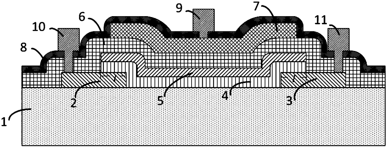
[0026] The structural schematic diagram of the thin film transistor based on the zinc oxide thin film of this embodiment is as follows figure 1 As shown, a structure of top gate and staggered electrodes is adopted, and from bottom to top, it includes substrate 1, source 2 and drain 3, semiconductor channel layer 4, first insulating layer 5, second insulating layer 6, and gate 7 in sequence. And the passivation insulating layer 8, the shape of the first insulating layer 5 is consistent with the shape of the semiconductor channel layer 4, as a protective layer of the semiconductor channel layer 4, the source 2, drain 3 and gate 7 are respectively passed through the source metal lead 10. The drain metal lead 11 and the gate metal lea...


PUM

PropertyMeasurementUnit
thicknessaaaaaaaaaa
widthaaaaaaaaaa
thicknessaaaaaaaaaa

Abstract

The invention discloses a thin-film transistor based on a zinc oxide thin film. The thin-film transistor comprises a semiconductor channel layer, gate insulating layers, a source electrode, a drain electrode and a gate electrode. According to the thin-film transistor based on the zinc oxide thin film, the zinc oxide thin film acts as the semiconductor channel layer, a top gate structure is adopted and the double gate insulating layers are adopted, and the first insulating layer of the gate insulating layers acts as the protective layer of the zinc oxide thin film so that the zinc oxide thin film can be effectively protected from being influenced by the environment or the subsequent technology. Multiple times of rapid annealing under the oxygen atmosphere is performed so that carrier concentration of the zinc oxide thin film can be effectively controlled and thus cut-off of the thin-film transistor can be realized under gate electrode bias voltage of being close to 0V. Besides, dehydrogenation processing is performed on the zinc oxide thin film, and the defects of the interface of the semiconductor channel layer and the insulating layers are restored so that electrical stability of the thin-film transistor can be greatly enhanced.

Description

Technical field [0001] The invention relates to the technical field of semiconductor devices, in particular to a thin film transistor based on a zinc oxide film. Background technique [0002] In recent years, with the rapid popularization of mobile terminals such as smart phones and tablet computers, and the continuous development of high-definition displays, people have increasingly higher requirements for display technology, such as large size, high contrast, high resolution, low power consumption, High opening rate and so on. Thin film transistors are used as pixel unit control switch components of liquid crystal panels (LCD) and organic light emitting diode (OLED) display panels, and their performance is critical to the impact of screen display technology. There are mainly two types of thin film transistors used in traditional liquid crystal panels. One is amorphous silicon thin film transistors. Because of their low cost and relatively mature technology, they are the most w...

Claims


Application Information

Patent Timeline
Patent Type & Authority Patents(China)
IPC IPC(8): H01L29/423H01L29/786
CPCH01L29/42364H01L29/7869
Inventor 叶志刘腾飞
Owner ZHEJIANG UNIV
Learn More