Method for preparing micro-nano PSS (Patterned Sapphire Substrate) by photoetching of nano flexible film

A kind of soft film, micro-nano technology, applied in the direction of nanotechnology, electrical components, circuits, etc., can solve the problems of poor exposure time, energy and other parameters, reduce the service life of the soft film, and long exposure time, etc., to achieve cost Low, improve work efficiency, high work efficiency effect

Inactive Publication Date: 2016-05-11
HAIDIKE NANTONG OPTOELECTRONICS TECH CO LTD
View PDF3 Cites 1 Cited by
  • Summary
  • Abstract
  • Description
  • Claims
  • Application Information

AI Technical Summary

Problems solved by technology

[0003] The preparation of micro-nano PSS includes the steps of uniform glue, exposure, development, etching, etc., but the traditional preparation method has the following disadvantages: the method of nanoimprinting is required for exposure, and this method requires the soft The film is in deep contact with the glue, and the soft film is generally made of resin, so it will cause the glue to pollute the soft film, and also reduce the service life of the soft film. Moreover, the traditional photolithography preparation method is not suitable for exposure time, energy, etc. The control of parameters is not very good, so step exposure is required, which leads to a long exposure time and low work efficiency

Method used


Image

  • Method for preparing micro-nano PSS (Patterned Sapphire Substrate) by photoetching of nano flexible film
  • Method for preparing micro-nano PSS (Patterned Sapphire Substrate) by photoetching of nano flexible film
  • Method for preparing micro-nano PSS (Patterned Sapphire Substrate) by photoetching of nano flexible film

Examples


Embodiment 1

[0023] The method for preparing micro-nano PSS by nano soft film lithography in the present invention is realized through the following steps:

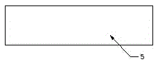
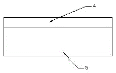
[0024] The first step, uniform glue: first, get a sapphire substrate 5, such as figure 1 As shown, a layer of photoresist 4 is evenly coated on the base layer of the sapphire substrate 5, such as figure 2 As shown, the thickness of the photoresist is between 1um. In this step, the photoresist can be a positive resist or a negative resist. This embodiment takes the positive resist as an example for further description.

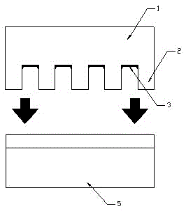
[0025] The second step, exposure: move the sapphire substrate under the soft film, such as image 3 As shown, the soft membrane includes a soft membrane main body 1, the soft membrane main body 1 is in the shape of a cuboid, and a comb group is arranged on one side of the long axis direction of the soft membrane main body 1. Teeth 2 are jointly formed, and a highly reflective metal layer 3 is also provided on the i...

Embodiment 2

[0029] The method for preparing micro-nano PSS by nano soft film lithography in the present invention is realized through the following steps:

[0030] The first step, uniform glue: first, get a sapphire substrate 5, evenly coat one deck photoresist 4 on the base layer of sapphire substrate 5, the thickness of photoresist is 1.1um, in this step, photoetching The glue can be a positive glue or a negative glue. In this embodiment, the positive glue is taken as an example for further description.

[0031] The second step, exposure: move the sapphire substrate to the bottom of the soft film, the soft film includes a soft film main body 10, the soft film main body 10 is in the shape of a cuboid, a comb is arranged on one side of the long axis direction of the soft film main body 10 The tooth group, the comb tooth group is composed of a number of parallel and equidistant comb teeth, and a high reflective metal layer 11 is also provided on the inner wall of the groove formed by two a...


PUM

PropertyMeasurementUnit
thicknessaaaaaaaaaa

Abstract

The invention relates to a method for preparing a micro-nano PSS (Patterned Sapphire Substrate) by photoetching of a nano flexible film. The method comprises the following steps: homogenizing glue: firstly, taking a sapphire substrate and uniformly coating a base layer of the sapphire substrate with one layer of photoresist; exposing: then, transferring the sapphire substrate to the lower side of the flexible film; enabling the soft film and the sapphire substrate to be in slight contact and carrying out exposure treatment; developing: moving the exposed sapphire substrate from the lower side of the flexible film, removing the exposed photoresist and remaining an unexposed part to realize pattern transferring; and etching: carrying out ICP etching treatment on the unexposed part of the photoresist so as to prepare the micro-nano PSS. The method provided by the invention has the advantages that when the method is used for preparing, the flexible film only needs to be in the slight contact with the photoresist, so that the pollution to the flexible film by the photoresist is effectively reduced and the service life of the flexible film is correspondingly prolonged; stepping type exposure does not need to be carried out and a whole wafer is molded in one step; and the method is suitable for preparing the large-size PSSs and the efficiency is relatively high.

Description

technical field [0001] The invention relates to the field of chip manufacturing, in particular to a method for preparing micro-nano PSS by photolithography of nano soft film. Background technique [0002] Light-emitting diode (LED) is a kind of electro-optic conversion, high efficiency and energy saving, green environmental protection, long life, etc. Solid-state lighting, which is expected to become a new generation of light source and enter thousands of households, will cause a revolution in the history of human lighting. Among them, the blue LED chip grown on the sapphire substrate with gallium nitride epitaxy is coated with yellow light phosphor, and the blue light excites the phosphor to emit yellow light. Blue light is mixed with yellow light to get white light, so blue LEDs are used to get white light. There are two common gallium nitride substrate materials, namely sapphire and silicon carbide. The poor machining performance of silicon carbide, high price and patent...

Claims


Application Information

Patent Timeline
Patent Type & Authority Applications(China)
IPC IPC(8): H01L33/22B82Y40/00
CPCH01L33/22B82Y40/00
Inventor 张伟孙智江
Owner HAIDIKE NANTONG OPTOELECTRONICS TECH CO LTD
Why Eureka
Try Eureka