Structure for improving the coupling efficiency between submicron silicon waveguide and common single-mode fiber

A common single-mode optical fiber and coupling efficiency technology, which is applied in the structural field of improving the coupling efficiency of sub-micron silicon waveguides and ordinary single-mode optical fibers, can solve the problems of small coupling tolerance, difficulty in packaging with devices, and high cost, and achieve a reduction in Fresnel effect of reducing reflection loss and reducing mode mismatch loss

Active Publication Date: 2016-05-25
宏芯科技(泉州)有限公司
View PDF5 Cites 16 Cited by
  • Summary
  • Abstract
  • Description
  • Claims
  • Application Information

AI Technical Summary

Problems solved by technology

The coupling loss of direct butt coupling between the two is above 10dB, which is unacceptable in practical applications
However, this approach can only increase the mode field of the silicon waveguide to a limited extent, and it is still necessary to use a tapered fiber with a small mode field to couple with the waveguide inverted cone structure. The cost is high and the coupling tolerance is small, so it is difficult to be used in the packaging of actual devices.

Method used


Image

  • Structure for improving the coupling efficiency between submicron silicon waveguide and common single-mode fiber
  • Structure for improving the coupling efficiency between submicron silicon waveguide and common single-mode fiber
  • Structure for improving the coupling efficiency between submicron silicon waveguide and common single-mode fiber

Examples


Embodiment Construction

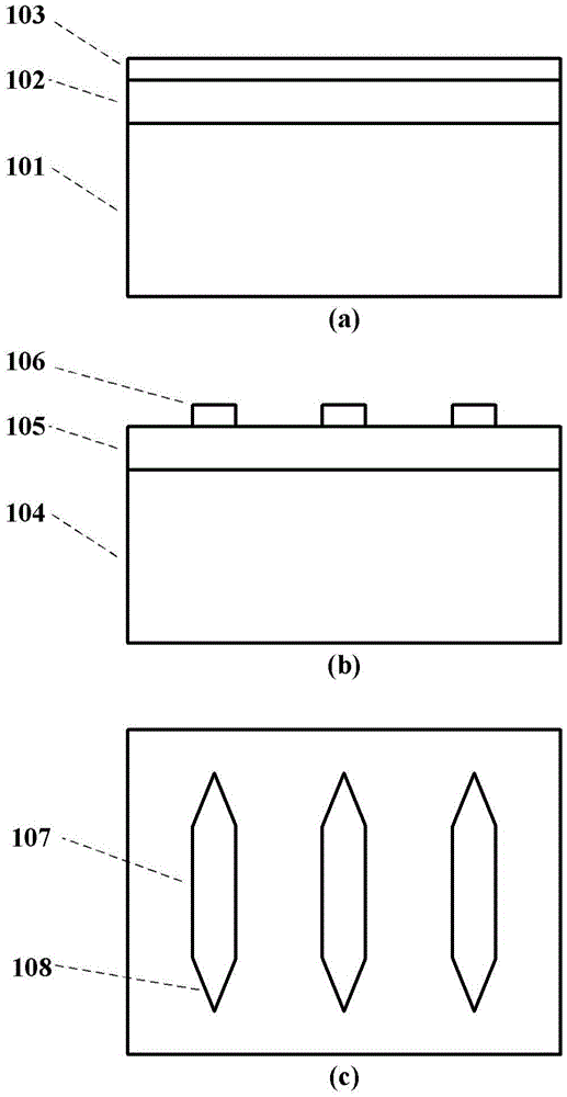
[0035] figure 1 (a) is a silicon wafer on an insulating substrate, which includes the following structures from bottom to top:

[0036] 101 is the substrate silicon structure, which is the lowermost layer of the three-layer structure of the silicon wafer on the insulating substrate. The material component is silicon, which can be pure silicon material or doped silicon material. It supports the whole The effect of wafer; 102 is the buried oxide layer structure, and it is the middle layer of the silicon wafer three-layer structure on the insulating substrate, and the buried oxide layer is doped silicon dioxide, and its material refractive index is higher than the material of pure silicon dioxide The refractive index is low, which can be achieved by doping elements such as boron or fluorine, and is used to form the lower cladding layer of the silicon dioxide waveguide; 103 is the top layer silicon structure, which is the uppermost layer of the three-layer structure of the silicon...


PUM


Abstract

The invention discloses a structure for improving the coupling efficiency between a submicron silicon waveguide and a common single-mode fiber. In the structure, the substrate material for making a submicron silicon waveguide is a silicon wafer on an insulating substrate, and the silicon wafer includes three layers of materials from bottom to top: substrate silicon, a buried oxide layer and top silicon, wherein the buried oxide layer is doped silicon dioxide; after forming a submicron silicon waveguide on the top silicon of the wafer through photoetching and etching, the doped silicon dioxide in the first layer is deposited on the silicon waveguide and fully covers the silicon waveguide; and after the doped silicon dioxide in the layer is photoetched and etched, the doped silicon dioxide in the second layer is deposited on the silicon waveguide. Therefore, the formed silicon dioxide waveguide is used as a connection channel for a common single-mode fiber, so that the mode field mismatch loss and the reflection loss during the coupling process of the submicron silicon waveguide and the common single-mode fiber, and the coupling efficiency between the submicron silicon waveguide and the common single-mode fiber can be improved.

Description

technical field [0001] The invention relates to the technical field of optical fiber communication and integrated optics, in particular to a structure for improving the coupling efficiency of a submicron silicon waveguide and a common single-mode optical fiber. Background technique [0002] Due to the large bending radius of traditional silicon-based large-section waveguides (on the order of hundreds of microns to millimeters), it is difficult to integrate multiple optical functional devices on a single chip, which limits the development of large-scale integrated optical circuits. With the advancement of semiconductor planar processing technology, silicon waveguides with sub-micron cross-sectional dimensions began to appear, and their radii can be as small as several microns without significant loss. Submicron silicon waveguides have attracted widespread attention because of their potential high-integration characteristics. [0003] Since the cross-sectional area of ​​the s...

Claims


Application Information

Patent Timeline
Patent Type & Authority Applications(China)
IPC IPC(8): G02B6/122
CPCG02B6/122G02B2006/12061
Inventor 杨林贾浩张磊
Owner 宏芯科技(泉州)有限公司
Why Eureka
Try Eureka