A 3D memory chip

A memory chip and chip technology, applied in information storage, static memory, digital memory information, etc., can solve the problems that hinder the development of portability and miniaturization of smart devices, do not support memory interface protocols, and increase the difficulty of motherboard design. Achieve the effect of saving motherboard area, simplifying motherboard design, and simple structure

Active Publication Date: 2018-04-06
SHANGHAI CIYU INFORMATION TECH CO LTD
View PDF6 Cites 0 Cited by
  • Summary
  • Abstract
  • Description
  • Claims
  • Application Information

AI Technical Summary

Problems solved by technology

[0006] 1. The installation positions of MRAM and DRAM need to be set on the motherboard at the same time, which will occupy more motherboard area and hinder the development of portability and miniaturization of smart devices
[0007] 2. The current memory interface, such as DDR interface, is very cumbersome to route on the motherboard. More memory chips make the design of the motherboard more difficult.
Although adding Base Die / LogicDie is more conducive to memory management, it also increases manufacturing costs and does not support existing memory interface protocols (such as DDR protocol)

Method used


Image

  • A 3D memory chip
  • A 3D memory chip

Examples


Embodiment Construction
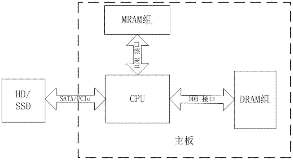
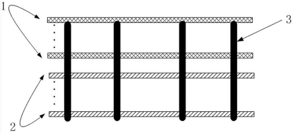
[0033] The design idea of ​​the present invention is based on 3D-SIC technology to use MRAM and DRAM in combination to form a memory chip with a 3D structure. In this embodiment, the combination of a 32-layer MRAM chip and a 32-layer DRAM chip is used as an example to illustrate the present invention. Detailed description.

[0034] The combined structure of MRAM and DRAM such as figure 2 As shown, the 32-layer MRAM chip 1 (2 layers are shown in the figure, and the dotted lines indicate the remaining unshown layers) and the 32-layer DRAM chip 2 (the 2 layers are shown in the figure, and the dotted lines indicate the remaining unshown layers) Each layer) is vertically stacked, and the DRAM chip 2 is located below the MRAM chip 1 . Each MRAM chip 1 and DRAM chip 2 adopts the DDR DRAM interface standard, and through silicon vias 3, the same defined lead pins in each MRAM chip 1 and DRAM chip 2 are connected in series to their corresponding package pins (not shown in the figure)....


PUM


Abstract

The invention discloses a 3D memory chip. An MRAM (Magnetic Random Access Memory) and a DRAM (Dynamic Random Access Memory) are subjected to mixed use based on a 3D-SIC (3D-Stacked Integrated Circuit) technology to form the 3D memory chip. The 3D memory chip comprises N stacked MRAM chips and M stacked DRAM chips, wherein N is a positive integer and M is a non negative integer; the MRAM chips and the DRAM chips are stacked in the same direction; the MRAM chips and the DRAM chips all adopt DDRDRAM (Double Data Rate Dynamic Random Access Memory) interface standards; and the same lead pins in all the MRAM chips and all the DRAM chips are electrically connected to the same package pin by through silicon vias. On this basis, the invention furthermore provides a multi-chip gating mechanism capable of effectively controlling the chip select signal line quantity.

Description

technical field [0001] The invention relates to a semiconductor memory, in particular to a 3D memory chip. Background technique [0002] In the current computer architecture, software and user data are stored in a hard disk (HD) or a new solid-state drive (SSD, using NAND Flash as a storage medium). The latter is connected to the computer motherboard through serial interfaces such as SATA and PCIe. Computing tasks are performed between the CPU and the memory (such as DRAM), and the communication between the two is carried out through a standard interface protocol (such as the DDR protocol). The packaged memory chips are generally mounted on the main board by patch, or combined into a memory bar and inserted into the corresponding slot provided on the main board. [0003] With the rapid development of computer application technology, the demand for memory performance and capacity is also increasing. [0004] At present, a new type of memory—Magnetic Random Access Memory (M...

Claims


Application Information

Patent Timeline
Patent Type & Authority Patents(China)
IPC IPC(8): G11C11/15G11C11/406
CPCG11C11/16
Inventor 戴瑾
Owner SHANGHAI CIYU INFORMATION TECH CO LTD
Why Eureka
Try Eureka