Trench gate power MOSFET (metal oxide semiconductor filed-effect transistor) device

A device and power technology, applied in the field of trench-gate power MOSFET devices, can solve the problems of difficult process and achieve the effects of increasing doping concentration, reducing power consumption, and increasing channel density

Active Publication Date: 2016-06-01
UNIV OF ELECTRONICS SCI & TECH OF CHINA
View PDF3 Cites 17 Cited by
  • Summary
  • Abstract
  • Description
  • Claims
  • Application Information

AI Technical Summary

Problems solved by technology

However, the P buried layer is formed by high-energy ion implantation, and the process is relatively difficult. At the same time, the P buried layer will also introduce the JFET (Junction Field-Effect-Transistor) effect.

Method used


Image

  • Trench gate power MOSFET (metal oxide semiconductor filed-effect transistor) device
  • Trench gate power MOSFET (metal oxide semiconductor filed-effect transistor) device
  • Trench gate power MOSFET (metal oxide semiconductor filed-effect transistor) device

Examples


Embodiment 1

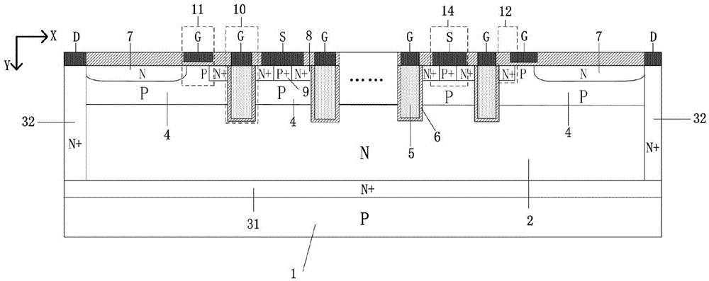
[0028] Such as figure 1 As mentioned above, it is a schematic diagram of the structure of the trench gate power MOSFET in Embodiment 1. This example includes the semiconductor substrate 1 of the second conductivity type and the heavily doped semiconductor drain region 31 of the first conductivity type above it; the heavily doped semiconductor of the first conductivity type Above the hetero-semiconductor drain region 31 is the semiconductor active layer 2 of the first conductivity type; the semiconductor body region 4 of the second conductivity type is arranged on the surface of the semiconductor active layer 2 of the first conductivity type. figure 2 It is a top view of the structure of this example. Depend on figure 1 and figure 2It can be seen from the figure that multiple columns of parallel trench gate structures 10 extend from the surface of the semiconductor body region 4 of the second conductivity type to the active layer 2 of the semiconductor of the first conducti...

Embodiment 2

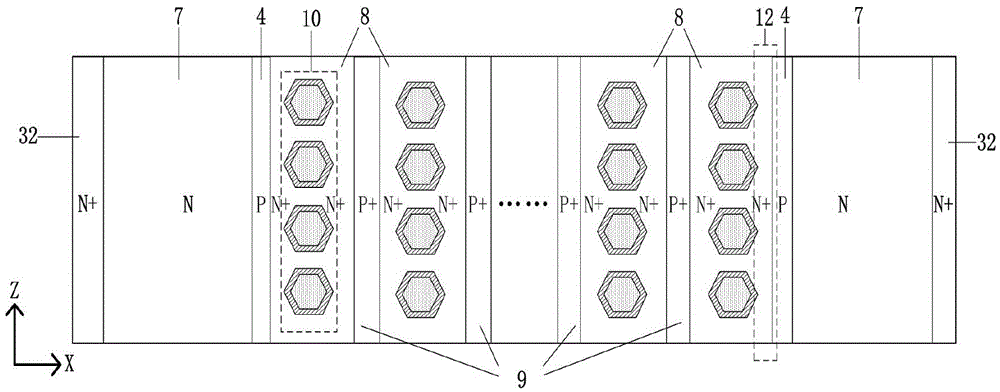
[0031] Such as image 3 As shown, the difference between this example and Example 1 is that the trench gate structure 10 is polygonal or circular in shape in a top view. The polygonal or circular trench gate can increase the current flow area and improve the current capacity.

Embodiment 3

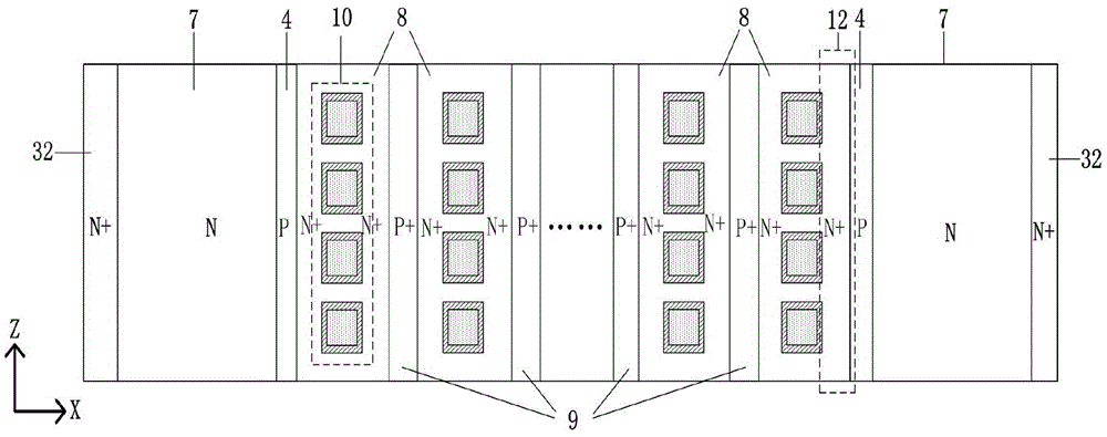
[0033] Such as Figure 4 As shown, the difference between the structure of this example and that of Example 1 is that the trench gate source structure 14 is longitudinally composed of segmented heavily doped semiconductor source regions 8 of the first conductivity type and the second conductivity type A heavily doped semiconductor body contact region 9 of the second conductivity type is formed, and the heavily doped semiconductor body contact region 9 of the second conductivity type is surrounded by a heavily doped semiconductor source region 8 of the first conductivity type. Figure 5 It is a cross-sectional view along AA' (half cell) of this example. It can be seen from the figure that the size of the device is further reduced, thereby effectively reducing the specific on-resistance of the device.


PUM


Abstract

The invention belongs to the technical field of a power semiconductor, and particularly relates to a trench gate power MOSFET (metal oxide semiconductor filed-effect transistor) device. The trench gate power MOSFET device has the following characteristics: 1, a crosswise heavily-doped semiconductor drain region and a longitudinal drain extension region are adopted, so that the device integrates the advantages of a VDMOS that can generate high current in a shunt-wound manner and a LDMOS that can be integrated easily; 2, a segmentation trench gate structure is adopted, so that the trench density can be improved, the device dimension can be saved, and the specific conduction resistance of the device can be lowered; and 3, RESURF structures are formed in the semiconductor region and a crosswise drift region, so that the surface electric field of the device can be improved, and the doping concentration of the crosswise drift region can be improved; and meanwhile, under a conduction state, a low-resistance channel is formed in the crosswise drift region, so that the power consumption of the device is dramatically lowered.

Description

technical field [0001] The invention belongs to the technical field of semiconductors, and in particular relates to a trench gate power MOSFET device. Background technique [0002] Power MOSFET (MetalOxide Semiconductor Filed-Effect Transistor) is a unipolar (multi-sub) conductive device with high input impedance, fast switching speed, easy drive, and compatibility with CMOS technology. It is used in computers, communications, new energy, rail transit, and smart grids. Widely used in other fields. [0003] Power VDMOS has the characteristics of parallel connection and can generate large current. At the same time, its cell size does not increase with the increase of withstand voltage, so that the device has a small specific on-resistance Ron.sp. However, there is a problem that power VDMOS cannot be integrated, which also limits its application in power integrated circuits. [0004] Power LDMOS is widely used in power integrated circuits due to the advantages of easy integr...

Claims


Application Information

Patent Timeline
Patent Type & Authority Applications(China)
IPC IPC(8): H01L29/423H01L29/78
CPCH01L29/4236H01L29/7801
Inventor 罗小蓉吕孟山尹超张彦辉马达吴俊峰阮新亮葛薇薇
Owner UNIV OF ELECTRONICS SCI & TECH OF CHINA
Why Eureka
Try Eureka