Manufacture method of die roller used for impressing electrode micro-grid films

A manufacturing method and technology of mold rolls, applied in the direction of using liquid cleaning methods, cleaning methods and utensils, chemical instruments and methods, etc., can solve the problem of unclear, uniform and inconsistent electrode micro-grid patterns on the surface of mold rolls, and difficulty in vertical pattern splicing To achieve seamless splicing, unable to meet the imprinting requirements and other problems, to achieve the effect of clear and consistent graphics, excellent mechanical strength and hardness, and low production cost

Active Publication Date: 2016-06-15
NANTONG VEEYEE NEW MATERIAL TECH CO LTD
View PDF6 Cites 3 Cited by
  • Summary
  • Abstract
  • Description
  • Claims
  • Application Information

AI Technical Summary

Problems solved by technology

[0005] Although round pressing and roll-to-roll embossing methods can significantly improve the productivity and format of conductive films, this embossing method also has certain defects: it is relatively difficult to prepare mold rolls with electrode micro-grid patterns. The graphics are made on the mold roll by mask exposure etching, which leads to unclear and inconsistent micro-grid patterns on the surface of the mold roll, which cannot meet the imprinting requirements. This process also has the disadvantages of high production cost and low input-output rate. At the same time, it is difficult for this process to make a big breakthrough in horizontal width, and it is also difficult to achieve seamless splicing in vertical graphics

Method used


Image

  • Manufacture method of die roller used for impressing electrode micro-grid films
  • Manufacture method of die roller used for impressing electrode micro-grid films
  • Manufacture method of die roller used for impressing electrode micro-grid films

Examples


Embodiment 1

[0022] The manufacturing method of the mold roll of the imprinted electrode micro-grid film in this embodiment, the specific steps of the manufacturing method are as follows:

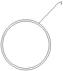
[0023] (1) if figure 1 As shown, a layer of masking glue with a thickness of 2 μm is coated on the outer surface of the mold roll;

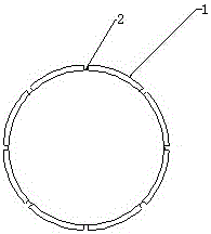
[0024] (2) if figure 2 As shown in the figure, the masking glue layer is etched away by direct writing with a laser direct writing device until it reaches the metal surface of the mold roll, and a groove-shaped electrode microgrid pattern 2 with a width of 5um and a height of 2μm is formed on the mold roll, using a 3W short-wavelength 266nm laser , the line scanning speed is 500mm / s, and the masking glue can be etched away in a few milliseconds;

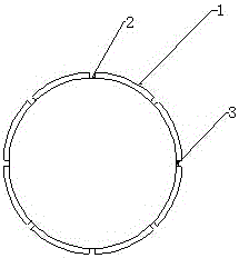
[0025] (3) if image 3 As shown, the mold roll after photoetching is cleaned with ultrasonic water to remove the masking glue remaining on the electrode micro-grid pattern and the slight metal oxide residue on the surface of...

Embodiment 2

[0028] The manufacturing method of the mold roll of the imprinted electrode micro-grid film in this embodiment, the specific steps of the manufacturing method are as follows:

[0029] (1) if figure 1 As shown, a layer of masking glue with a thickness of 3 μm is coated on the outer surface of the mold roll;

[0030] (2) if figure 2 As shown, the masking glue layer is etched away by direct writing with a laser direct writing device until it reaches the metal surface of the mold roll, and a groove-shaped electrode microgrid pattern 2 with a width of 4um and a height of 3μm is formed on the mold roll, using a 3W short-wavelength 266nm laser , the line scanning speed is 500mm / s, and the masking glue can be etched away in a few milliseconds;

[0031] (3) if image 3 As shown, the mold roll after photoetching is cleaned with ultrasonic water to remove the masking glue remaining on the electrode micro-grid pattern and the slight metal oxide residue on the surface of the mold roll...

Embodiment 3

[0034] The manufacturing method of the mold roll of the imprinted electrode micro-grid film in this embodiment, the specific steps of the manufacturing method are as follows:

[0035] (1) if figure 1 As shown, a layer of masking glue with a thickness of 4 μm is coated on the outer surface of the mold roll;

[0036] (2) if figure 2 As shown, the masking glue layer is etched away by direct writing with a laser direct writing device until it reaches the metal surface of the mold roll, and a groove-shaped electrode microgrid pattern 2 with a width of 5um and a height of 4μm is formed on the mold roll, using a 3W short-wavelength 266nm laser , the line scanning speed is 500mm / s, and the masking glue can be etched away in a few milliseconds;

[0037] (3) if image 3 As shown, the mold roll after photoetching is cleaned with ultrasonic water to remove the masking glue remaining on the electrode micro-grid pattern and the slight metal oxide residue on the surface of the mold roll...


PUM

PropertyMeasurementUnit
thicknessaaaaaaaaaa
lengthaaaaaaaaaa

Abstract

The invention relates to a manufacture method of a die roller used for impressing electrode micro-grid films. The die roller is manufactured by the manufacture method by the following steps: coating a masking adhesive, carrying out laser direct writing photoetching on the masking adhesive, ultrasonically washing and electrodepositing. The manufacture method has the advantages that through controlling special technical conditions and parameters about laser photoetching, ultrasonic washing and electro-deposition in the manufacture process, electrode micro-grid patterns on the surface of the die roller manufactured are kept clear and consistent; and through the manufacture method, the die roller manufactured is high in input-output ratio but low in manufacture cost.

Description

technical field [0001] The invention belongs to the technical field of mold roll processing of conductive films, and in particular relates to a method for manufacturing a mold roll for embossing electrode microgrid films. Background technique [0002] Conductive film is a new material that appears with the development of magnetron sputtering technology. It can achieve some specific electronic and physical properties. The square resistance is 5-500ohm and the thickness is 0.05-0.25mm. Inherent electrical properties; thus, a key component in flat panel and touch screen displays. [0003] The traditional conductive film is a planar embossing technology, and its format is determined by the size of the printed board. Its utilization rate is low when it is cut and used in the later stage, which greatly wastes resources and increases the cost; [0004] After the improvement, it adopts the method of round pressing and roll-to-roll embossing. The mold roll with electrode micro-grid ...

Claims


Application Information

Patent Timeline
Patent Type & Authority Applications(China)
IPC IPC(8): B29C59/04B08B3/12B23K26/362C25D5/02
CPCB08B3/12B29C59/04C25D5/022
Inventor 邱晓华王新辉
Owner NANTONG VEEYEE NEW MATERIAL TECH CO LTD
Why Eureka
Try Eureka