
Epitaxial structure of light emitting diode and epitaxial growth method therefor

A technology of light-emitting diodes and epitaxial growth, applied in electrical components, circuits, semiconductor devices, etc., can solve problems such as poor anti-static ability of LEDs, and achieve the effect of improving anti-static ability, slowing defects and dislocations, and reducing leakage channels

Inactive Publication Date: 2016-06-15
HC SEMITEK SUZHOU
View PDF4 Cites 6 Cited by
  • Summary
  • Abstract
  • Description
  • Claims
  • Application Information

AI Technical Summary

Problems solved by technology

[0004] In order to solve the problem of poor antistatic ability of LED caused by a large number of dislocations in the prior art, an embodiment of the present invention provides an epitaxial structure and an epitaxial growth method of a light emitting diode

Method used


Image

  • Epitaxial structure of light emitting diode and epitaxial growth method therefor
  • Epitaxial structure of light emitting diode and epitaxial growth method therefor
  • Epitaxial structure of light emitting diode and epitaxial growth method therefor

Examples


Embodiment 1

[0037] An embodiment of the present invention provides an epitaxial structure of a light emitting diode, see figure 1 , the epitaxial structure includes a sapphire substrate 1, and Al stacked sequentially on the sapphire substrate 1 x Ga 1-x N buffer layer 2, GaN buffer layer 3, undoped GaN layer 4, N-type GaN layer 5, shallow well layer 6, multiple quantum well layer 7, low-temperature P-type GaN layer 8, P-type AlGaN electron blocking layer 9, high temperature For the P-type GaN layer 10 and the P-type GaN contact layer 11, 0.3≦x≦0.8.

[0038] In this embodiment, both the shallow well layer 6 and the multiple quantum well layer 7 include alternately stacked InGaN layers and GaN layers.

[0039] Optionally, Al x Ga 1-x The thickness of the N buffer layer 2 may be 2-8 nm. When Al x Ga 1-x When the thickness of the N buffer layer 2 is less than 2nm, it cannot effectively alleviate the Al 2 o 3 Lattice mismatch between GaN and GaN; when Al x Ga 1-x When the thickness ...

Embodiment 2

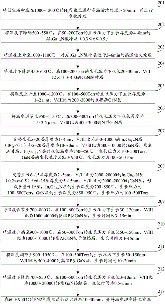
[0054] An embodiment of the present invention provides an epitaxial growth method of a light emitting diode, which is a specific implementation of the epitaxial structure of a light emitting diode provided in Embodiment 1, see figure 2 , the epitaxial growth method includes:

[0055] Step 201: Put the sapphire substrate in H at 1000-1200°C 2 Carry out high-temperature cleaning treatment in the atmosphere for 5-20 minutes, and carry out nitriding treatment.

[0056] Step 202: Lower the temperature to 500-550° C., and grow Al with a thickness of 4-8 nm under a growth pressure of 50-200 Torr x Ga 1-x N buffer layer (0.3≤x≤0.5).

[0057] Step 203: raise the temperature to 1000-1100°C, for Al x Ga 1-x The N buffer layer is subjected to high-temperature annealing treatment for 3-6 minutes.

[0058] Step 204: Lower the temperature to 450-600° C., and grow a GaN buffer layer with a thickness of 20-30 nm and a V / III ratio of 100-400 under a growth pressure of 100-200 Torr.

[0...

Embodiment 3

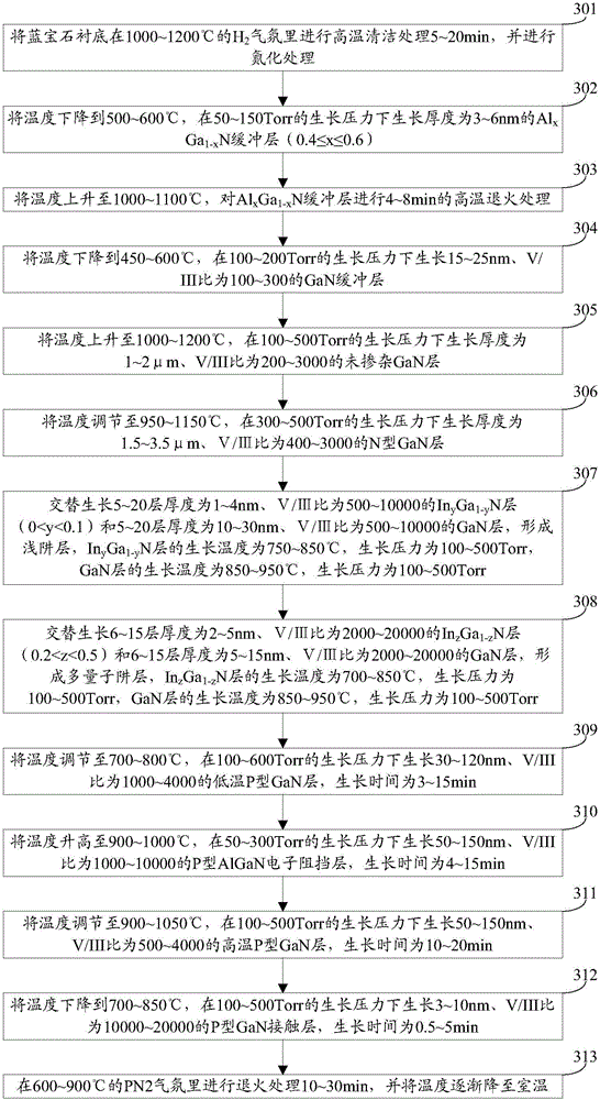
[0070] An embodiment of the present invention provides an epitaxial growth method of a light-emitting diode, which is another specific realization of the epitaxial structure of a light-emitting diode provided in Embodiment 1, see image 3 , the epitaxial growth method includes:

[0071] Step 301: Put the sapphire substrate in H at 1000-1200°C 2 Carry out high-temperature cleaning treatment in the atmosphere for 5-20 minutes, and carry out nitriding treatment.

[0072] Step 302: Lower the temperature to 500-600° C., and grow Al with a thickness of 3-6 nm under a growth pressure of 50-150 Torr x Ga 1-x N buffer layer (0.4≤x≤0.6).

[0073] Step 303: Raise the temperature to 1000-1100°C, for Al x Ga 1-x The N buffer layer is subjected to high-temperature annealing treatment for 4-8 minutes.

[0074] Step 304: Lower the temperature to 450-600° C., and grow a GaN buffer layer with a thickness of 15-25 nm and a V / III ratio of 100-300 under a growth pressure of 100-200 Torr.

...


PUM


Abstract

The invention discloses an epitaxial structure of a light emitting diode and an epitaxial growth method therefor, and belongs to the technical field of a semiconductor. The epitaxial structure comprises a sapphire substrate, and a GaN buffer layer, a un-doped GaN layer, an N type GaN layer, a shallow well layer, a multi-quantum-well layer, a low-temperature P type GaN layer, a P type AlGaN electron barrier layer, a high-temperature P type GaN layer and a P type GaN contact layer that are laminated on the sapphire substrate in sequence, wherein the epitaxial structure also comprises an AlxGa1-xN buffer layer laminated between the sapphire substrate and the GaN buffer layer; and x is greater than or equal to 0.3 and less than or equal to 0.8. According to the epitaxial structure, the AlxGa1-xN buffer layer is arranged between the sapphire substrate taking Al2O3 as the main ingredient, and the GaN buffer layer, so that defects and dislocation caused by lattice mismatch between the Al2O3 and GaN can be effectively relieved, the electric leakage channels of the light emitting diode are reduced, and the anti-static capability of the light emitting diode is improved.

Description

technical field [0001] The invention relates to the technical field of semiconductors, in particular to an epitaxial structure and an epitaxial growth method of a light emitting diode. Background technique [0002] The core part of a light-emitting diode (LightEmittingDiode, referred to as LED) is a wafer composed of a P-type semiconductor and an N-type semiconductor. There is a transition layer between the P-type semiconductor and the N-type semiconductor, which is called a PN junction. In the PN junction of some semiconductor materials, when the injected holes and electrons recombine, the excess energy will be released in the form of light, thereby directly converting electrical energy into light energy. [0003] At present, 80% of the substrates used in the production of GaN-based LEDs use sapphire (Al 2 o 3 ) substrate, however Al 2 o 3 The lattice mismatch and thermal expansion coefficient of GaN are very different. During the epitaxial growth process, a large numbe...

Claims


Application Information

Patent Timeline
Patent Type & Authority Applications(China)
IPC IPC(8): H01L33/00H01L33/06H01L33/12H01L33/32
CPCH01L33/32H01L33/0075H01L33/06H01L33/12
Inventor 肖云飞
Owner HC SEMITEK SUZHOU
Learn More