Nano-particle material, and light-emitting device

一种纳米粒子、发光器件的技术,应用在发光器件领域,能够解决材料制约大、成本提高、制造工序工序增加等问题,达到阻挡性能提高、注入效率提高、驱动电压低的效果

Active Publication Date: 2016-06-15
MURATA MFG CO LTD
View PDF7 Cites 35 Cited by
  • Summary
  • Abstract
  • Description
  • Claims
  • Application Information

AI Technical Summary

Problems solved by technology

[0037] However, in Figure 26 In the light-emitting device, it is necessary to newly provide a hole blocking layer 134 between the quantum dots 131 and the electron transport layer 133, which may increase the number of steps in the manufacturing process and increase the cost.
In addition, since the hole blocking layer 134 needs to have a predetermined energy level as described above in order to efficiently block holes so that the holes do not leak to the outside, and requires electron transport properties, material constraints are also large, and there may be a possibility of new subject

Method used


Image

  • Nano-particle material, and light-emitting device
  • Nano-particle material, and light-emitting device
  • Nano-particle material, and light-emitting device

Examples


no. 1 approach 〕

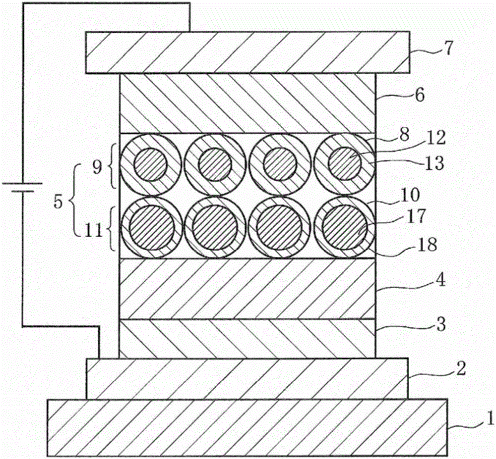
[0098] figure 1 It is a cross-sectional view schematically showing a first embodiment of an EL element as a light-emitting device according to the present invention, and the light-emitting layer is formed of the nanoparticle material according to the present invention.

[0099] In this EL element, an anode 2 is formed on a transparent substrate 1 such as a glass substrate, and a hole injection layer 3 and a hole transport layer 4 formed of a hole transport material are sequentially formed on the surface of the anode 2. The surface of the layer 4 is formed with a light emitting layer 5 . In addition, an electron transport layer 6 made of an electron transport material is formed on the surface of the light emitting layer 5 , and a cathode 7 is formed on the surface of the electron transport layer 6 .

[0100] The light-emitting layer 5 becomes a first light-emitting layer 9 having first quantum dots 8 arranged vertically and horizontally as the nanoparticle material of the pre...

no. 2 approach 〕

[0184] Figure 8 It is a cross-sectional view schematically showing a second embodiment of an EL element as a light emitting device according to the present invention.

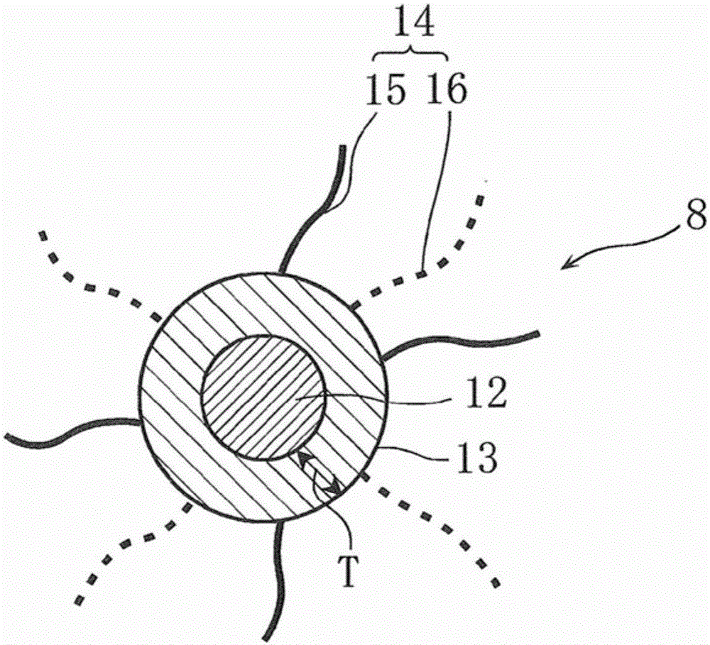
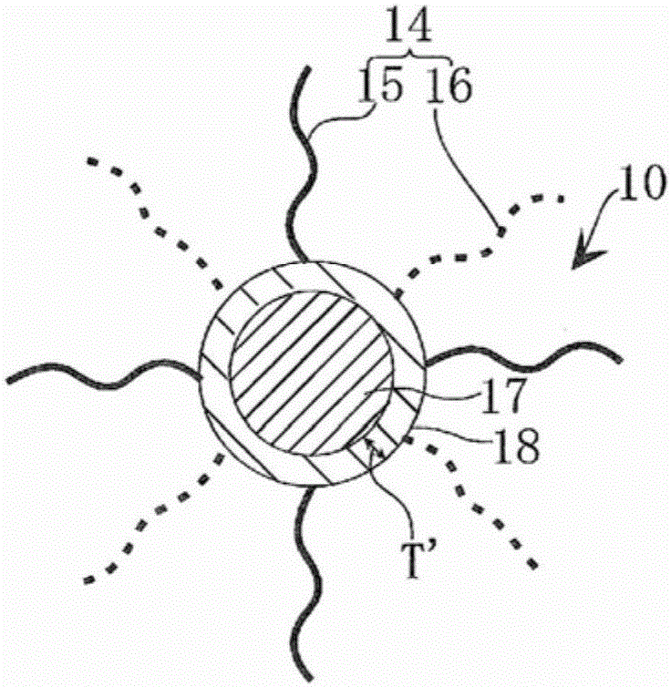
[0185] In this EL element, the light-emitting layer 24 has a laminated structure of a first light-emitting layer 25 formed of first quantum dots 27 and a second light-emitting layer 26 formed of second quantum dots 10 . Furthermore, in the second quantum dot 10, the shell portion 18 is covered with the respective surfactants having hole-transporting and electron-transporting properties, while in the first quantum dot 27, the shell portion 13 is only transported by electrons. Active surfactant coverage.

[0186] That is, in this second embodiment, the first quantum dot 27 such as Figure 9 As shown, it has a core-shell structure including a core part 12 and a shell part 13. The surface of the shell part 13 is covered only by the second surfactant 16 having electron transport properties. The thickness T of the...

no. 3 approach 〕

[0204] Figure 12 It is a cross-sectional view schematically showing a third embodiment of an EL element as a light emitting device according to the present invention.

[0205] In this EL element, the light-emitting layer 30 has a laminated structure of a first light-emitting layer 31 formed of first quantum dots 33 and a second light-emitting layer 32 formed of second quantum dots 10 . Furthermore, the second quantum dots 10 are covered with the respective surfactants having hole-transporting properties and electron-transporting properties, while the first quantum dots 33 are covered with insulating surfactants.

[0206] That is, in this third embodiment, the first quantum dot 33 such as Figure 13 As shown, it has a core-shell structure including a core part 12 and a shell part 13. The surface of the shell part 13 is covered with an insulating third surfactant 34. The thickness T of the shell part 13 is determined by the constituent molecules of the shell part 13. Benchmar...


PUM

PropertyMeasurementUnit
particle diameteraaaaaaaaaa
concentrationaaaaaaaaaa

Abstract

A first quantum dot (8) has a core (12) and a shell (13), the surface of the shell (13) is coated with a surfactant, and the thickness of the shell (13) is 3-5 ML expressed in terms of the molecules constituting the shell (13). A second quantum dot (10) has a core (17) and a shell (18); the surface of the shell (18) is coated with two types of surfactants, one having a hole-transport property and one having an electron-transport property; and the thickness of the shell (18) is less than 3 ML expressed in terms of the molecules constituting the shell (18). A first light-emitting layer (9) is formed by the first quantum dots (8) and a second light-emitting layer (11) is formed by the second quantum dots (10). This minimizes external leaking of holes and increases the probability of recombination while maintaining the efficiency with which a carrier is injected into the nano-particle material, so as to yield a nano-particle material suitable as a light-emitting device material able to emit light at high efficiency, and a light-emitting device in which this nano-particle material is used in the light-emitting layer.

Description

technical field [0001] The present invention relates to a nanoparticle material and a light-emitting device, and more specifically, to a nanoparticle material having a core-shell structure, and a light-emitting device such as an EL element (EL: ElectroLuminescence) in which a light-emitting layer is formed using the nanoparticle material. Background technique [0002] Since quantum dots, which are nanoparticles having a particle size of 10 nm or less, are excellent in confinement of carriers (electrons and holes), excitons can be easily generated by recombination of electrons and holes. Therefore, light emission from free excitons can be expected, and light emission with high light emission efficiency and a sharp light emission spectrum can be realized. In addition, since quantum dots can realize control over a wide wavelength range utilizing the quantum size effect, applications to light-emitting devices such as EL elements, light-emitting diodes (LEDs), and semiconductor l...

Claims


Application Information

Patent Timeline
Patent Type & Authority Applications(China)
IPC IPC(8): H05B33/14B82Y20/00C09K11/00C09K11/08H01L51/50
CPCB82Y20/00C09K11/025C09K11/565C09K11/883H10K85/1135H10K85/324H10K50/115H10K50/13H10K2102/351H10K50/17H10K50/11H10K50/15H10K50/16H10K71/12H10K71/164H10K85/111H10K85/151H10K2101/40H10K2101/30
Inventor 村山浩二宫田晴哉
Owner MURATA MFG CO LTD
Why Eureka
Try Eureka