Optical filter based on graphene

An optical filter device and graphene technology, applied in the direction of instruments, optics, nonlinear optics, etc., can solve the problems of small quality factor, non-tunable, high loss, etc., and achieve the effect of large quality factor, reduced size, and low power consumption

Inactive Publication Date: 2016-06-22
CENTRAL SOUTH UNIVERSITY OF FORESTRY AND TECHNOLOGY
View PDF4 Cites 13 Cited by
  • Summary
  • Abstract
  • Description
  • Claims
  • Application Information

AI Technical Summary

Problems solved by technology

[0003] Traditional optical filter devices have disadvantages such as high loss, small quality factor, large size, and non-tunable

Method used


Image

  • Optical filter based on graphene
  • Optical filter based on graphene
  • Optical filter based on graphene

Examples


Embodiment 1

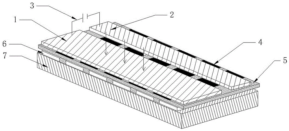
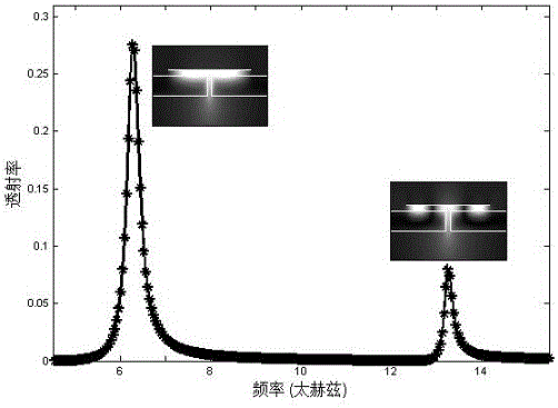
[0028] A beam of parallel light with a wavelength in the infrared band is vertically incident on the electrolyte layer, and the incident light is TM mode (the magnetic field component is perpendicular to the incident surface). The thickness of the electrolyte layer and the metal electrode is 300nm, the period of the graphene strip array and the metal grating is 8000nm or 8 microns, the bandwidth of the graphene strip in the graphene strip array is 720nm, and the gap width of two adjacent metal strips in the metal grating The thickness of silicon dioxide dielectric, metal grating and substrate silicon carbide are 20, 80 and 500nm respectively. The carrier mobility and Fermi velocity of graphene are 20000 cm 2 / (Vs) and 10 6 m / s, the metal grating in this embodiment is a gold grating, and a silver grating can be used in other embodiments. Adjust the top gate voltage V g Let the Fermi level of graphene be 0.6eV. Under the above parameters, it can be obtained as figure 2 The...

Embodiment 2

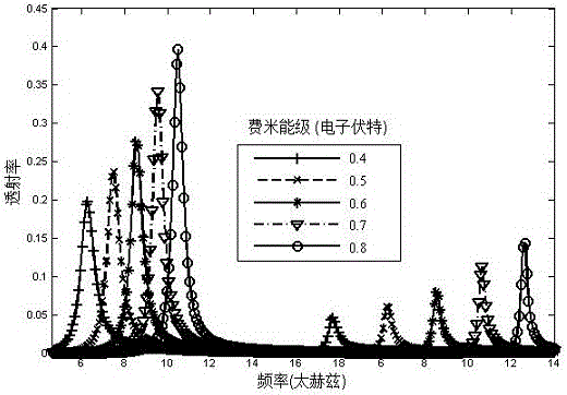
[0031] The Fermi level of graphene can pass the top gate voltage V g Make adjustments. The change of the Fermi level of graphene leads to the change of the coupled electromagnetic mode propagation constant (effective refractive index) of the Fabry-Perot microcavity, which changes the response frequency of the microcavity. image 3 is the transmission spectrum at different Fermi levels (other parameters are the same as in Example 1). When the Fermi level of graphene increases from 0.4eV to 0.8eV, the two transmission peaks on the left and right are blue-shifted, the magnitudes of the blue shifts are 2.1 and 4.5THz, and the speeds of the blue shifts are 0.53 and 1.12THz / eV, respectively. The two transmission peaks increase as the Fermi level increases, and the quality factor increases accordingly. When the Fermi level reaches 0.8 electron volts, the quality factors of the left and right transmission peaks reach 28 and 89, respectively.


PUM

PropertyMeasurementUnit
widthaaaaaaaaaa
thicknessaaaaaaaaaa
widthaaaaaaaaaa

Abstract

An optical filter based on graphene comprises an optical coupling structure. The optical coupling structure comprises an electrolyte layer, a metal electrode, a graphene strip array, a dielectric layer, a metal optical grating and a substrate. The electrolyte layer and the metal electrode are provided with adjusting devices for top gate voltage. A Fabry-Perot microcavity array composed of the graphene strip array, the dielectric layer and the metal optical grating is located on the substrate, and the electrolyte layer and the metal electrode are located on the same plane above the Fabry-Perot microcavity. Based on the micro-nano etching process technology and the multiplayer film technology which are extremely mature at present, the technological process is not complex, and operation is easy. Compared with a traditional filter with the same frequency band, the optical filter has the advantage that the size of a coupled component is greatly reduced due to introduction of graphene. The optical filter frequency is regulated by adjusting the Fermi level of graphene through grid voltage, active control over light is achieved, the needed power consumption is small, the quality factor is large, the response speed is high, and very wide working frequency is achieved.

Description

technical field [0001] The invention relates to a filter device, in particular to a graphene-based optical filter device. Background technique [0002] Graphene is a two-dimensional crystal composed of carbon atoms with only one atomic thickness. It has an ultra-broadband optical response spectrum, strong nonlinear optical properties, and compatibility with silicon-based semiconductor processes, making it suitable for new optical and The field of optoelectronic devices has unique advantages. Under certain conditions, graphene surface conduction electrons interact with photons to form coupled electromagnetic modes (ie, surface plasmons). The coupled electromagnetic mode has strong locality, can break through the diffraction limit, and can be used as an information carrier in an optical coupling device. The biggest advantage of coupled electromagnetic modes is that their propagation constants can be adjusted by external electric (or magnetic) or chemical doping. [0003] Tr...

Claims


Application Information

Patent Timeline
Patent Type & Authority Applications(China)
IPC IPC(8): G02F1/00G02F1/01
CPCG02F1/0009G02F1/01
Inventor 贺梦冬彭宇翔王凯军
Owner CENTRAL SOUTH UNIVERSITY OF FORESTRY AND TECHNOLOGY
Why Eureka
Try Eureka