Circuit structure used for driving silicon-based avalanche photodiode

An avalanche photoelectric and circuit structure technology, which is applied in the direction of logic circuits using optoelectronic devices, logic circuits using specific components, logic circuits, etc., can solve the problems of high power consumption, low response speed, and large dark current of control circuits. Low power consumption, fast response, and low circuit noise

Inactive Publication Date: 2016-08-03
合肥汇芯半导体科技有限公司
View PDF5 Cites 3 Cited by
  • Summary
  • Abstract
  • Description
  • Claims
  • Application Information

AI Technical Summary

Problems solved by technology

[0007] The technical problem to be solved by the present invention is to provide a circuit structure for driving silicon-based avalanche photodiodes. , high power consumption of the control circuit and other problems mentioned above

Method used


Image

  • Circuit structure used for driving silicon-based avalanche photodiode
  • Circuit structure used for driving silicon-based avalanche photodiode

Examples


Embodiment Construction

[0023] In order to make the technical means, creative features, goals and effects achieved by the present invention easy to understand, the present invention will be further described below in conjunction with specific illustrations.

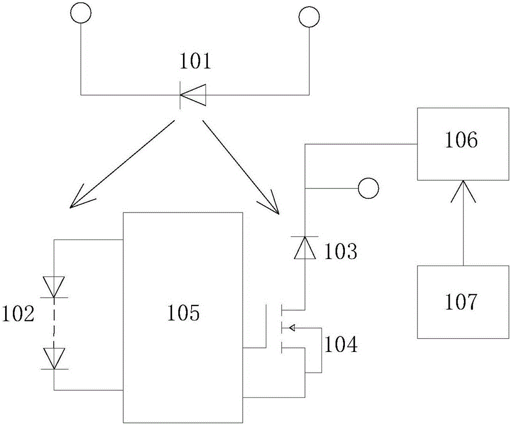
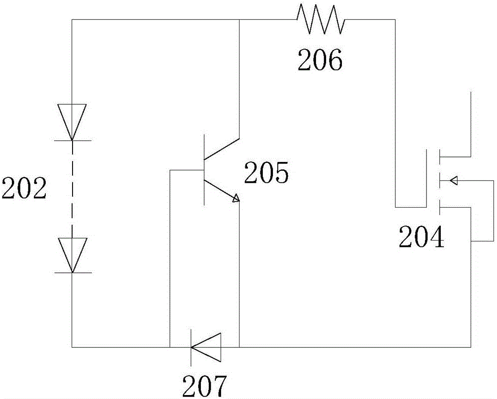
[0024] Such as figure 1 As shown, a circuit structure for driving a silicon-based avalanche photodiode, which includes a diode; the diode includes a photovoltaic diode array 102 and a silicon-based avalanche photodiode 103, and the circuit structure also includes a charge and discharge management circuit 105, a field effect Transistor 104, high-voltage bias circuit 106 and bias voltage setting circuit 107; The photovoltaic diode array 102 is used to generate photovoltaic output voltage in response to light signals; the two ends of the input terminal of the charge and discharge management circuit 105 are connected to the positive and negative poles of the photovoltaic diode array 102 The two ends of the output terminal of the charge and discharge...


PUM


Abstract

The invention relates to a circuit structure for driving a silicon-based avalanche photodiode, which includes a photovoltaic diode array, a silicon-based avalanche photodiode, a charge and discharge management circuit, a field effect transistor, a high-voltage bias circuit and a bias voltage setting circuit; The two ends of the input end of the charging and discharging management circuit are connected to the positive and negative poles of the photovoltaic diode array; the two ends of the output end of the charging and discharging management circuit are connected to the gate and source of the field effect transistor; The drains of the effect transistors are connected; the output end of the high-voltage bias circuit is connected with the cathode of the silicon-based avalanche photodiode, and the output end of the bias voltage setting circuit is connected with the input end of the high-voltage bias circuit; the beneficial effects of the present invention are: the The response speed of the circuit structure is fast, the dark current is extremely low when there is no light, the light-current gain is high, the control circuit has a good isolation effect, the circuit power consumption is low, and the circuit structure is relatively simple.

Description

technical field [0001] The invention relates to a circuit structure, in particular to a circuit structure for driving silicon-based avalanche photodiodes. Background technique [0002] An optoelectronic integrated circuit refers to an integrated circuit that integrates optoelectronic devices and microelectronic devices on the same substrate to achieve a specific function. It greatly eliminates the negative parasitic effects in traditional circuits and reduces hybrid circuits. In the assembly link, the electrical signal output by the electronic device is converted into an optical signal with excellent multiplexing ability, lower transmission loss, stronger anti-interference performance and better transmission speed, because these remarkable characteristics are widely used in Optical fiber communication, optical control radar system, optical disc system, medical system, laser ranging and photoelectric detection and other fields. Silicon-based optoelectronic integrated circuit...

Claims


Application Information

Patent Timeline
Patent Type & Authority Applications(China)
IPC IPC(8): H03K19/14H03K19/094H03K19/00
CPCH03K19/14H03K19/0013H03K19/094
Inventor 谢峰
Owner 合肥汇芯半导体科技有限公司
Why Eureka
Try Eureka