

Photosensitive ink and electromagnetic shielding structure employing same, circuit board, and electronic device
A technology of electromagnetic shielding structure and photosensitive ink, which is applied in the fields of magnetic/electric field shielding, ink, application, etc., and can solve the problems of expensive silver and long curing time of conductive ink
- Summary
- Abstract
- Description
- Claims
- Application Information
AI Technical Summary
Problems solved by technology
Method used
Image

Examples
Embodiment 1
[0031] In this embodiment, the photosensitive ink is composed of aromatic urethane resin, tripropylene glycol diacrylate, 1-hydroxycyclohexyl phenyl ketone, palladium acetate, isophorone and hydroxyethyl acrylate. Wherein the massfraction of aromatic urethane resin is 45%, the massfraction of tripropylene glycol diacrylate is 20%, the massfraction of 1-hydroxycyclohexyl phenyl ketone is 2%, the massfraction of palladium acetate The fraction is 1%, the mass fraction of isophorone is 30%, and the mass fraction of hydroxyethyl acrylate is 2%.
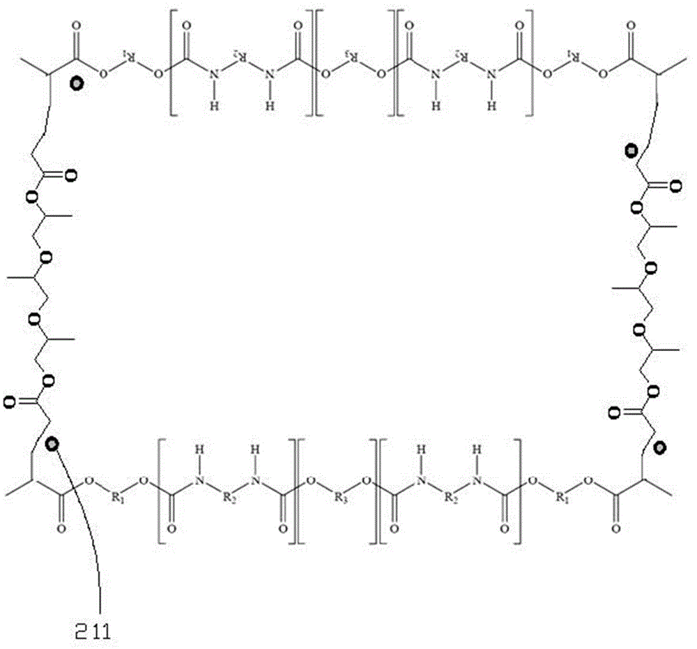
[0032] The general structural formula of the aromatic urethane resin is
[0033]
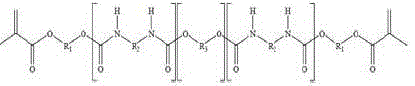
[0034] Among them, R 1 is a carbon-carbon double bond (C=C), R 2 One of the following structural formulas:-(CH 2 -CH 2 -O), , , , , , R 3 for H or CH 3 .
[0035] The structural formula of described tripropylene glycol diacrylate is
[0036] .
[0037] The structural formula of the 1-hydroxycyclohexyl phenyl ketone is
[0038] .
...
Embodiment 2
[0047] In this embodiment, the photosensitive ink is composed of urethane acrylate, hexafunctional aliphatic urethane acrylate, dimethylammonia-oxazetidinone, palladium acetate, isophorone and polydimethylsiloxane. Wherein the massfraction of urethane acrylate is 55%, the massfraction of hexafunctional aliphatic urethane acrylate is 15%, the massfraction of dimethylammonium-oxazeridone is 2%, and the massfraction of palladium acetate is 1 %, the mass fraction of isophorone is 25%, and the mass fraction of polydimethylsiloxane is 2%.
Embodiment 3
[0049] In this embodiment, the photosensitive ink is composed of polyether acrylate, tripropylene glycol methyl ether monoacrylate, 1-hydroxycyclohexyl phenyl ketone, palladium chloride, cyclohexane and polydimethylsiloxane. Wherein, the mass fraction of polyether acrylate is 20%, the mass fraction of tripropylene glycol methyl ether monoacrylate is 50%, the mass fraction of 1-hydroxycyclohexyl phenyl ketone is 4%, the mass fraction of palladium chloride The mass fraction of cyclohexane is 21%, and the mass fraction of polydimethylsiloxane is 3%.
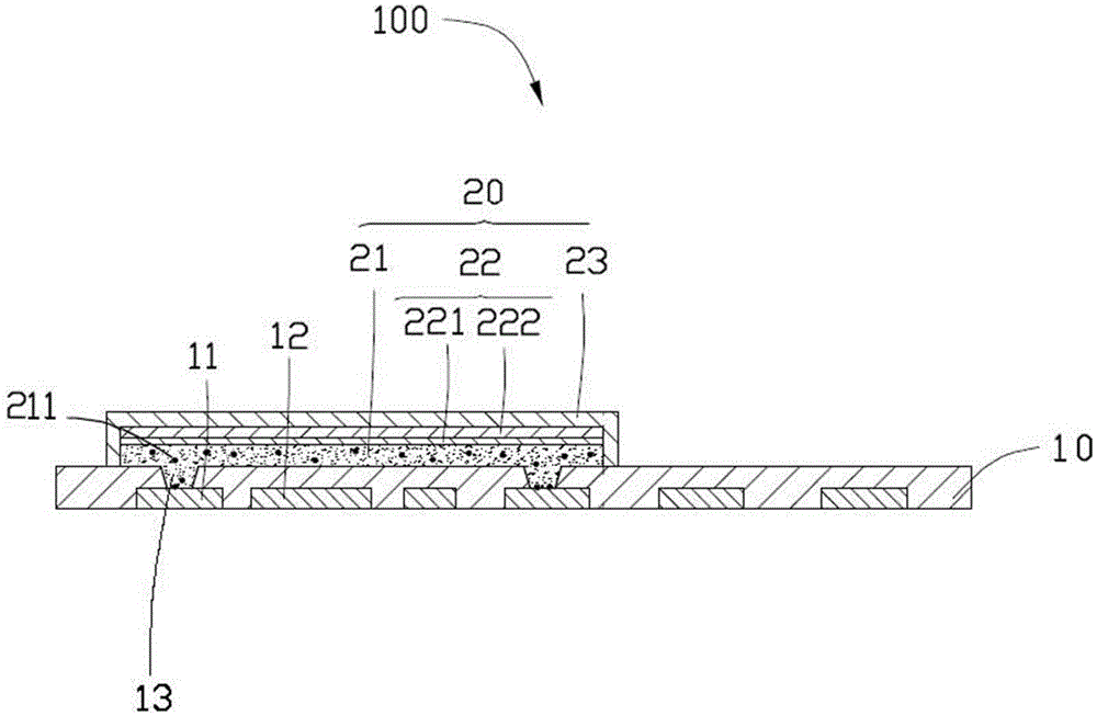
[0050] When using the photosensitive ink, the photosensitive ink is first coated on the surface of a substrate (not shown in the figure), and then irradiated with ultraviolet light. Under the irradiation of ultraviolet light, the photoinitiator generates an initial reaction free radical, which attacks the photosensitive monomer to form a reaction unit, and the reaction unit then attacks the double bond of the photosensitive oligomer...
PUM
 Abstract
Description
Claims
Application Information