
Radiation-resistant double interlock memory cell for dynamic voltage adjustment system

A dynamic voltage adjustment, storage unit technology, applied in static memory, information storage, digital memory information, etc., can solve the problems of DICE type storage unit limitation, data loss, voltage increase, etc., to optimize delay and power consumption, reduce Soft error rate, the effect of enhancing stability

Active Publication Date: 2018-12-07
XI AN JIAOTONG UNIV
View PDF5 Cites 0 Cited by
  • Summary
  • Abstract
  • Description
  • Claims
  • Application Information

AI Technical Summary

Problems solved by technology

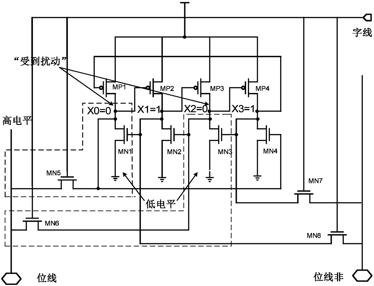
like figure 1 As shown, in the dotted line box shown in the figure, two groups of "ratio circuits" are formed by MN5 and MN1, MN6 and MN3. Assuming that the nodes X0 and X2 are at low level at this time, before the read operation starts, the bit line and the bit line The line is not precharged to a high level, and then the word line is turned on. At the moment when the word line is turned on, the voltage of X0 and X2 will suddenly rise
If the boosted voltage reaches the threshold voltage of MN2 and MN4, the positive feedback structure inside the entire unit will be triggered, resulting in data loss, which is called "read destruction".
It is because of this phenomenon that the DICE type memory cell is limited in the application field of low voltage and low power consumption.
So far, there are few studies on the stability of DICE memory cells under low voltage.

Method used


Image

  • Radiation-resistant double interlock memory cell for dynamic voltage adjustment system
  • Radiation-resistant double interlock memory cell for dynamic voltage adjustment system
  • Radiation-resistant double interlock memory cell for dynamic voltage adjustment system

Examples


Embodiment Construction

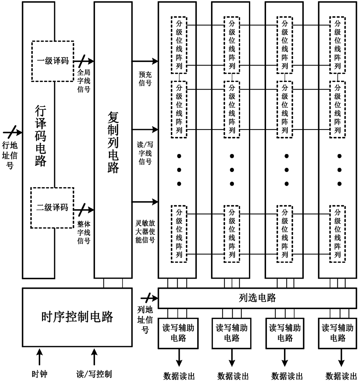
[0025] see figure 2 As shown, the overall circuit structure diagram of the SRAM of the embodiment of the present invention includes: row / column decoding circuit; SRAM storage cell array; read and write auxiliary circuit; copy column circuit; timing control circuit; wherein, row / column decoding The circuit selects the corresponding memory cell through the address signal, and at the same time, the timing control circuit starts to perform virtual read / write operations on the replicated column, generates a pre-fill signal and a word line pulse signal of a suitable width, and a sense amplifier turn-on signal, and These signals are sent to the SRAM memory array for actual read / write operations. Take the read operation as an example, assuming that the stored data of the selected cell is 0 at this time, the read word line signal comes, the read word line of the selected cell becomes high level, and the read bit line starts to discharge. Usually, the sensitive amplifier in the read-w...


PUM


Abstract

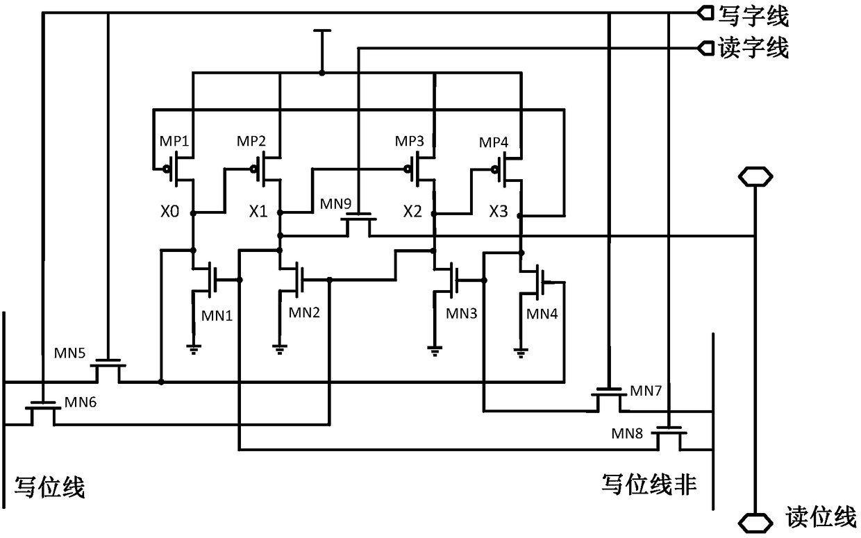
The invention discloses a radiation-proof DICE memory cell applied to a DVS system. An original DICE cell is provided with a read tube MN9, a read word line for controlling MN9 conduction, and a read bit line connected with a sensitive amplifier; above modification makes one and only one memory node be disturbed by a bit line partial pressure when the read word line starts; and disturbance to a single node automatically recovers after a disturbance source disappears by using the "binode feedback" structural characteristic of the DICE cell, and data stored in the memory cell is not affected, so the "read destroy" phenomenon is eliminated. The structure of the DICE cell becomes connection of the read bit line with one memory node from connection of the read bit line with two in-phase nodes, solves the problem of simultaneous overturning of the two in-phase nodes, induced by the bit line partial pressure when the word line starts, guarantees normal read of data, and improves the robustness of the memory cell in the subthreshold working process.

Description

technical field [0001] The invention relates to a semiconductor integrated circuit, in particular to a storage unit structure used for a static random access memory SRAM (Static Random Access Memory). Background technique [0002] Radiation-resistant SRAM has attracted much attention in the aerospace field and has always been a research hotspot. When low-energy α particles emitted from packaging materials and high-energy heavy ions in space are incident on integrated circuit MOS devices, energy will be deposited at sensitive nodes inside the device, and the phenomenon of "Single Event Upset (SEU)" will appear. "Upset Hardened Memory Design for Submicron CMOS Technology" published on TRANSACTIONSON NUCLEAR SCIENCE in 1996 proposed a DICE (Dual Interlocked Storage cell) structure storage unit for deep submicron technology to reduce the occurrence of single event flipping , to reduce the soft error rate of SRAM. The DICE unit uses 4 nodes to represent a bit of binary data sto...

Claims


Application Information

Patent Timeline
Patent Type & Authority Patents(China)
IPC IPC(8): G11C11/412
CPCG11C11/4125
Inventor 耿莉李广林张杰商中夏宋璐雯苗孟涛
Owner XI AN JIAOTONG UNIV
Learn More