Method for realizing enhanced HEMT (High Electron Mobility Transistor) by virtue of p-type passivation and enhanced HEMT

An enhanced, p-type technology, applied in the field of microelectronics technology, can solve problems such as affecting device stability, reducing device performance, and small saturation current, achieving the effects of low cost, reduced interface state, and high repeatability

Inactive Publication Date: 2016-08-17
SUZHOU NENGWU ELECTRONICS TECH
View PDF4 Cites 17 Cited by
  • Summary
  • Abstract
  • Description
  • Claims
  • Application Information

AI Technical Summary

Problems solved by technology

The concave gate structure solves the problem of small saturation current, but the barrier layer in the general HEMT device is only 20-30nm, and the process of forming the concave gate structure by etching process is difficult to control and the repeatability is poor
For another example, F plasma treatment can also realize enhanced HEMT devices, and does not require etching, but F plasma will also etch the barrier layer during the implantation process, resulting in a decrease in device performance
The p-type cap layer also requires an etching process, which is difficult to control and has poor repeatability. At the same time, an interface state is generated, which affects the stability of the device.

Method used


Image

  • Method for realizing enhanced HEMT (High Electron Mobility Transistor) by virtue of p-type passivation and enhanced HEMT
  • Method for realizing enhanced HEMT (High Electron Mobility Transistor) by virtue of p-type passivation and enhanced HEMT
  • Method for realizing enhanced HEMT (High Electron Mobility Transistor) by virtue of p-type passivation and enhanced HEMT

Examples


Embodiment 1

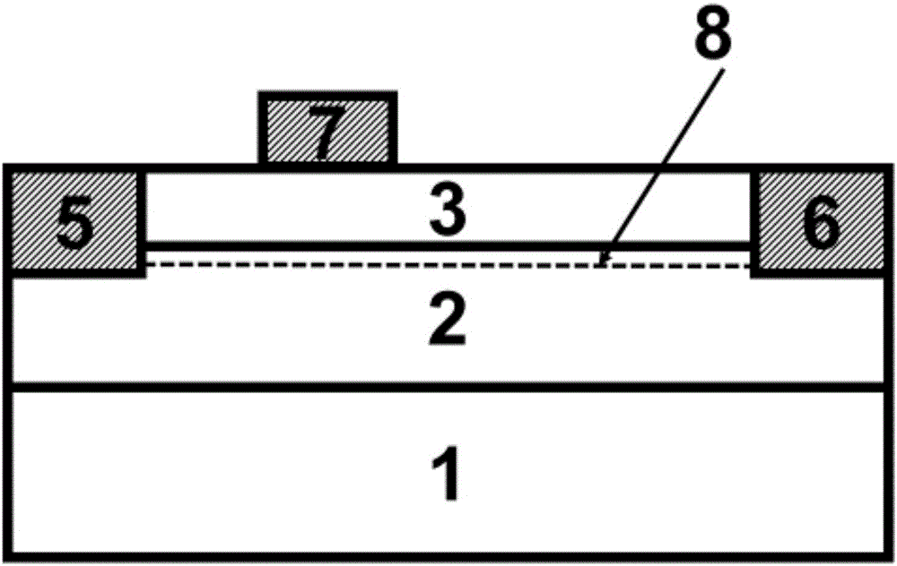
[0063] Example 1: Please refer to Figure 4 A method for fabricating an enhanced HEMT by implanting H ions into a p-type doped layer according to this embodiment includes the following steps:

[0064] (1) Treat the substrate surface in the reaction chamber of the epitaxial growth equipment;

[0065] (2) Epitaxial growth of AlGaN / GaN epitaxial layer and p-GaN on the substrate, wherein the thickness of GaN is 1μm-3μm, the thickness of AlGaN is 14nm-30nm, and the molar content of Al element is 20%-30%, p -GaN thickness is 5-100nm, Mg doping concentration is 10 16 After being taken out from the chamber, it is cleaned with an organic solution and purged with high-purity nitrogen;

[0066] (3) Photolithographic development is carried out on the cleaned sample, the photoresist is AZ5214, the exposure time is 6.5s, the development time is 50s-60s, and the table is isolated, and ion implantation or plasma etching can be used;

[0067] (4) By photolithography, etch the source and dra...

Embodiment 2

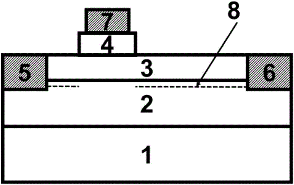
[0071] see again Figure 4 A method of manufacturing an enhanced HEMT realized by implanting H ions into a P-type doped layer comprises the following steps:

[0072] (1) processing the substrate surface in the reaction chamber;

[0073] (2) Epitaxial growth of AlGaN / GaN epitaxial layer and p-GaN on the substrate, wherein the thickness of GaN is 1μm-3μm, the thickness of AlGaN is 14nm-30nm, and the molar content of Al element is 20%-30%, p -GaN thickness is 5-100nm, Mg doping concentration is 10 16 After being taken out from the chamber, it is cleaned with an organic solution and purged with high-purity nitrogen;

[0074] (3) Photolithographic development is carried out to the cleaned sample. The photoresist is AZ5214, the exposure time is 6.5s, and the development time is 50s-60s. Use the photoresist as a mask and use an ion implanter to implant H ions. H can effectively combine with Mg in the implanted region of the p-type doped layer, making it lose the p-type characteris...


PUM


Abstract

The invention discloses a method for realizing an enhanced HEMT (High Electron Mobility Transistor) by virtue of p-type passivation. The method comprises the following steps: providing a heterostructure which mainly comprises a first semiconductor and a second semiconductor, wherein the second semiconductor is distributed on the first semiconductor and is provided with a band gap wider than the first semiconductor, and two-dimensional electron gas is formed in the heterostructure; forming a p-type doped third semiconductor on the second semiconductor, performing passivation treatment on a residual region, except for an under-gate region, of the third semiconductor, so that the p-type doped region only exists at the under-gate region, and the under-gate region is distributed under a gate electrode of an HEMT device; manufacturing a source electrode, a drain electrode and a gate electrode connected with the heterostructure, electrically connecting the source electrode and the drain electrode through the two-dimensional electron gas, and enabling the gate electrode to be distributed between the source electrode and the drain electrode. The invention further discloses the enhanced HEMT. The method has the advantages of simple process, high repeatability, stable and favorable device performance, low cost, easiness for large-scale production and the like.

Description

technical field [0001] The invention relates to an enhanced HEMT (high electron mobility transistor) device and a preparation method thereof, in particular to a method for realizing an enhanced HEMT through p-type passivation and the enhanced HEMT formed thereby, belonging to the field of microelectronic technology. Background technique [0002] HEMT devices are made by making full use of the two-dimensional electron gas formed by the semiconductor heterostructure (Heterostructure) structure. Compared with III-VI (such as AlGaAs / GaAs HEMT), III-nitride semiconductors are due to piezoelectric polarization And the spontaneous polarization effect, a high-concentration two-dimensional electron gas can be formed in the heterostructure (such as AlGaN / GaN). Therefore, in HEMT devices made of group III nitrides, the barrier layer generally does not need to be doped. At the same time, group III nitrides have the characteristics of large band gap, high saturated electron drift veloci...

Claims


Application Information

Patent Timeline
Patent Type & Authority Applications(China)
IPC IPC(8): H01L21/335H01L29/778H01L29/06
CPCH01L29/0603H01L29/66462H01L29/7787
Inventor 宋亮郝荣晖付凯张志利孙世闯李维毅李夏珺袁洁于国浩邓旭光范亚明蔡勇张宝顺
Owner SUZHOU NENGWU ELECTRONICS TECH
Why Eureka
Try Eureka