Infrared LED (Light-Emitting Diode)

A light-emitting diode and infrared light-emitting technology, applied in the field of optoelectronics, can solve the problems of high resistivity of materials, poor antistatic resistance of current diffusion components, etc., and achieve the effects of improving luminous efficiency, improving red burst phenomenon, and low resistivity

Active Publication Date: 2016-08-17
TIANJIN SANAN OPTOELECTRONICS
View PDF9 Cites 5 Cited by
  • Summary
  • Abstract
  • Description
  • Claims
  • Application Information

AI Technical Summary

Problems solved by technology

[0003] Generally, InGaAs is used as the multi-quantum well structure of the active layer. Infrared light-emitting diodes with a luminous peak wavelength above 900nm, the covering layer mostly uses AlGaAs with an indirect energy gap. Among them, Al is an atom with high activity and is easy to oxidize. Higher, making the current spread and the antistatic resistance of the component poor

Method used


Image

  • Infrared LED (Light-Emitting Diode)
  • Infrared LED (Light-Emitting Diode)

Examples


Embodiment 1

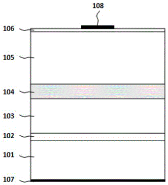
[0041] Such as figure 1 As shown, an infrared light-emitting diode chip with a low-bandgap covering layer includes, from top to bottom, a P-type ohmic electrode 108, a contact layer 106, a P-type covering layer 105, a quantum well active layer 104, and an N-type covering layer 103. , buffer layer 102, GaAs substrate 101, N-type ohmic electrode 107. In this embodiment, the multi-quantum well active layer is grown by metal-organic vapor phase epitaxy (OMVPE), with InGaAs as the well layer and AlGaAsP as the barrier layer. The luminescence peak wavelength is above 900nm, and the number of quantum wells is between Between 3 pairs and 25 pairs.

[0042] Specifically, the GaAs substrate 101 is a single crystal N-type GaAs substrate doped with Si, with a concentration of 8E17-3E18 atoms / cm, preferably 1.2E18 atoms / cm; the buffer layer 102 is made of GaAs, with a concentration of Between 8E17~5E18 atoms / cm, the preferred concentration is 1.5E18 atoms / cm; the N-type cladding layer is...

Embodiment 2

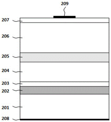
[0046] Such as figure 2 As shown, an infrared light-emitting diode chip with a low-bandgap covering layer includes, from top to bottom, an N-type ohmic electrode 209, an N-type contact layer 207, an N-type covering layer 206, an active layer 205, and a P-type covering layer 204. , P-type contact layer 203 , metal bonding layer 202 , Si substrate 201 and P-type ohmic electrode 208 . In this embodiment, a Si substrate is used, and a metal bonding layer is used to reflect downward light from the active layer, so as to effectively improve light extraction, thereby improving luminous efficiency.

[0047] Specifically, the N-type cladding layer 206 and the P-type cladding layer 204 are made of indium gallium arsenide In x Ga 1-x As, wherein the indium component X is between 0%~5%, preferably X is 2%, the concentration is 5E17~2E18 atoms / cm, and the preferred concentration is 7E17 atoms / cm. The active layer 205 is a multi-quantum well layer, including a well layer and a barrier l...


PUM


Abstract

The invention discloses an infrared LED (Light-Emitting Diode) which comprises a P-type ohmic electrode, a contact layer, a P-type coating layer, an active layer, an N-type coating layer, a buffer layer, a GaAs substrate and an N-type ohmic electrode. The infrared LED is characterized in that InxGa1-xAs is utilized as the N-type coating layer and the P-type coating layer or one of the N-type coating layer and the P-type coating layer. The infrared LED has the advantages that when InxGa1-xAs is utilized as the coating layer, current diffusion can be effectively improved by virtue of the low resistance of the material, the voltage is reduced, and the light-emitting efficiency is improved.

Description

technical field [0001] The invention belongs to the technical field of optoelectronics, and in particular relates to an infrared light-emitting diode which improves current diffusion and luminous efficiency. Background technique [0002] Due to its specific wavelength band, low power consumption and high reliability, infrared light-emitting diodes are widely used in security monitoring, wearable devices, space communication, remote control, medical appliances, light sources for sensors, and night lighting. [0003] Generally, InGaAs is used as the multi-quantum well structure of the active layer. Infrared light-emitting diodes with a luminous peak wavelength above 900nm, the covering layer mostly uses AlGaAs with an indirect energy gap. Among them, Al is an atom with high activity and is easy to oxidize. Higher, making the current spread and the antistatic resistance of the component poor. Contents of the invention [0004] In view of the foregoing problems, the present i...

Claims


Application Information

Patent Timeline
Patent Type & Authority Applications(China)
IPC IPC(8): H01L31/0304H01L31/0352
CPCH01L31/03042H01L31/03046H01L31/035236H01L33/405H01L33/12H01L33/30H01L33/0093H01L31/0304H01L31/0352H01L33/06H01L2933/0016
Inventor 黄俊凯吴俊毅王笃祥吴超瑜王进
Owner TIANJIN SANAN OPTOELECTRONICS
Why Eureka
Try Eureka