Resistance-type gas sensor based on graphene, stannic oxide and zinc oxide composite, preparation method and application thereof

A gas sensor, tin dioxide technology, applied in nanotechnology for materials and surface science, material resistance, analytical materials, etc., can solve problems such as hindering application, slow response recovery, low sensitivity, etc., to achieve easy operation, improve The effect of adhesion and high response sensitivity

Inactive Publication Date: 2016-08-24
JILIN UNIV
View PDF4 Cites 39 Cited by
  • Summary
  • Abstract
  • Description
  • Claims
  • Application Information

AI Technical Summary

Problems solved by technology

Although the detection of gases at room temperature has been realized, the composites of metal oxides and conductive polymers exhibit problems such as low sensitivity and slow response recovery, which seriously hinder their further application.

Method used


Image

  • Resistance-type gas sensor based on graphene, stannic oxide and zinc oxide composite, preparation method and application thereof
  • Resistance-type gas sensor based on graphene, stannic oxide and zinc oxide composite, preparation method and application thereof
  • Resistance-type gas sensor based on graphene, stannic oxide and zinc oxide composite, preparation method and application thereof

Examples


Embodiment 1

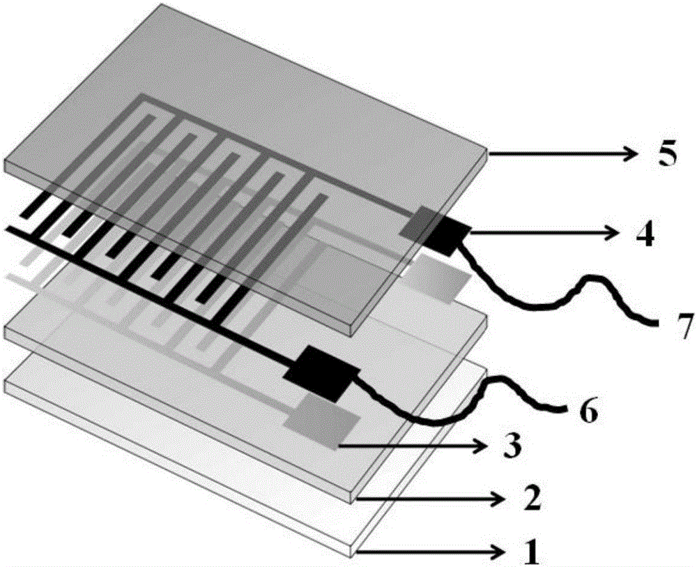
[0031](1) Using single crystal silicon as the substrate, a silicon dioxide layer is formed on the surface of the single crystal silicon by thermal oxidation, with a thickness of 150nm, and a titanium adhesion layer is deposited on the surface of silicon dioxide by magnetron sputtering, with a thickness of 40nm ; Deposit a platinum metal layer on the surface of the titanium adhesion layer by magnetron sputtering, with a thickness of 50nm; spin-coat BP212 (Kempur Microelectronic INC) positive photoresist on the surface of the platinum metal, with a thickness of 1 μm; The same photoresist plate is placed on the photoresist surface, exposed to 350W ultraviolet light for 15 minutes, and then developed with a sodium hydroxide solution with a mass fraction of 5 / 1000, and the exposed photoresist is removed after development; Argon ions are used to bombard the surface of the platinum metal layer and the titanium adhesion layer, and the platinum metal layer and the titanium adhesion laye...

Embodiment 2

[0037] (1) With monocrystalline silicon as the substrate, a silicon dioxide layer is formed on the surface of the monocrystalline silicon by thermal oxidation method, with a thickness of 180nm, and a titanium adhesion layer is deposited on the surface of silicon dioxide by magnetron sputtering, with a thickness of 60nm ; Deposit a platinum metal layer on the surface of the titanium adhesion layer by magnetron sputtering, with a thickness of 100nm; spin-coat BP212 (Kempur Microelectronic INC) positive photoresist on the surface of the platinum metal, with a thickness of 1 μm; The same photoresist plate is placed on the photoresist surface, exposed to 350W ultraviolet light for 15 minutes, and then developed with a sodium hydroxide solution with a mass fraction of 5 / 1000, and the exposed photoresist is removed after development; then Argon ions are used to bombard the surface of the platinum metal layer and the titanium adhesion layer, and the platinum metal layer and the titaniu...

Embodiment 3

[0043] (1) Using single crystal silicon as the substrate, a silicon dioxide layer is formed on the surface of the single crystal silicon by thermal oxidation, with a thickness of 210nm, and a titanium adhesion layer is deposited on the surface of silicon dioxide by magnetron sputtering, with a thickness of 60nm ; Deposit a platinum metal layer on the surface of the titanium adhesion layer by magnetron sputtering, with a thickness of 100nm; spin-coat BP212 (Kempur Microelectronic INC) positive photoresist on the surface of the platinum metal, with a thickness of 1 μm; The same photoresist plate is placed on the photoresist surface, exposed to 350W ultraviolet light for 15 minutes, and then developed with a sodium hydroxide solution with a mass fraction of 5 / 1000, and the exposed photoresist is removed after development; then Argon ions are used to bombard the surface of the platinum metal layer and the titanium adhesion layer, and the platinum metal layer and the titanium adhesi...


PUM

PropertyMeasurementUnit
sizeaaaaaaaaaa
specific surface areaaaaaaaaaaa
thicknessaaaaaaaaaa

Abstract

The invention relates to a resistance-type gas sensor based on a graphene, stannic oxide and zinc oxide composite, a preparation method and application thereof, and belongs to the technical field of gas sensors. The gas sensor is composed of a monocrystalline silicon substrate, a silicon dioxide layer, a titanium adhesion layer, interdigital platinum electrodes and a gas sensitive film covering the silicon dioxide layer and the surfaces of the interdigital platinum electrodes in sequence; the structure of the titanium adhesion layer is the same as that of the interdigital platinum electrodes, and the gas sensitive film is the graphene, stannic oxide and zinc oxide ternary composite; the ternary composite is prepared by mixing graphene, stannic oxide and zinc oxide and is of a three-dimensional porous structure. Before and after the gas sensitive film makes contact with gas to be tested, the resistance of the gas sensitive film can change, and the sensitivity of the sensor can be obtained by measuring resistance changes between the interdigital platinum electrodes. The sensor has high response sensitivity, rapid response recovery rate and good response reversibility at room temperature, and the problem that the a stannic oxide and zinc oxide gas sensor can work only at high temperature is solved.

Description

technical field [0001] The invention belongs to the technical field of gas sensors, in particular to a graphene-based resistance-type gas sensor with room temperature gas-sensitive response characteristics and a manufacturing method thereof, in particular to a resistance based on a graphene / tin dioxide / zinc oxide composite material Type gas sensor, preparation method and application thereof. Background technique [0002] With the rapid development of industry, agriculture and transportation, the problem of environmental pollution has become more and more prominent. Especially in recent years, the emission of toxic and harmful gases and flammable and explosive gases has been increasing day by day. Accurate and continuous detection of gases in the environment has become an urgent problem to be solved, which provides a broad space for the application of gas sensors. Gas sensors are an important class of chemical sensors, which are widely used in industrial and agricultural pro...

Claims


Application Information

Patent Timeline
Patent Type & Authority Applications(China)
IPC IPC(8): G01N27/12B82Y30/00B82Y40/00
CPCB82Y30/00B82Y40/00G01N27/127
Inventor 刘森王子莹张勇张彤
Owner JILIN UNIV
Why Eureka
Try Eureka