Bipolar resistive random access memory and preparation method thereof
A resistive memory, bipolar technology, applied in electrical components and other directions, can solve problems such as difficult and high-density three-dimensional integration, inability to take advantage of RRAM's scalability advantages, and inability to use RRAM.
- Summary
- Abstract
- Description
- Claims
- Application Information
AI Technical Summary
Problems solved by technology
Method used
Image
Examples
preparation example Construction
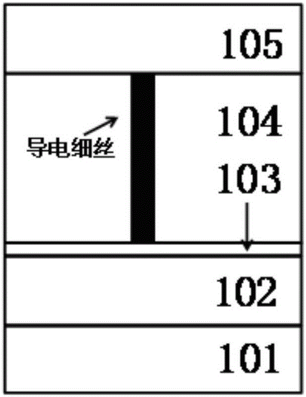
[0057] The present invention also provides a method for preparing the bipolar resistive memory, comprising: S1) providing a substrate; S2) forming a lower electrode on the upper surface of the substrate; S3) depositing rectification functional layer; the rectification functional layer is made of Al 2 o 3 、TiO 2 Forming with one or more of MgO; S4) transferring the graphene film to the rectification function layer to form a graphene layer; S5) depositing a resistive medium layer on the graphene layer; S6) forming a graphene layer on the graphene layer; An upper electrode is deposited on the resistive medium layer to obtain a bipolar resistive memory.
[0058] Wherein, the substrate, the lower electrode, the rectifying functional layer, the graphene layer, the resistive medium layer and the upper electrode are all the same as above, and will not be repeated here; see Figure 4 , Figure 4 It is a schematic diagram of the preparation process of the bipolar resistive memory of...
Embodiment 1
[0068] 1.1 Provide substrate SiO 2 / Si.
[0069] 1.2 Deposit metal Pt50nm and Ti10nm on the substrate as the bottom electrode by E-beam evaporation process.
[0070] 1.3 Deposit 3nm Al on the bottom electrode by magnetron sputtering 2 o 3 A rectification functional layer is formed.
[0071] 1.4 Transfer the single-layer graphene obtained by the chemical vapor deposition (CVD) process on the copper sheet to the rectifying functional layer to form a graphene layer by a peeling transfer process.
[0072] 1.5 Deposit 10nm HfO on the graphene layer by magnetron sputtering 2 As a resistive dielectric layer.
[0073] 1.6 Deposit 70nm metal Cu as the upper electrode on the resistive dielectric layer by electron beam evaporation process.
[0074] 1.7 Deposit 10nm metal Au as a protective layer on the upper electrode by electron beam evaporation process.
Embodiment 2
[0076] 2.1 Provide substrate SiO 2 / Si.
[0077] 2.2 Deposit metal Au50nm and Ti10nm on the substrate as the bottom electrode by E-beam evaporation process.
[0078] 2.3 Deposit 3nm MgO on the lower electrode by magnetron sputtering to form a rectifying functional layer.
[0079] 2.4 Transfer the bilayer graphene obtained by the chemical vapor deposition (CVD) process on the copper sheet to the rectifying functional layer to form a graphene layer by a peeling transfer process.
[0080] 2.5 Deposit 10nm ZrO on the graphene layer by magnetron sputtering 2 As a resistive dielectric layer.
[0081] 2.6 Deposit 70nm metal Ag on the resistive medium layer by electron beam evaporation process as the upper electrode.
[0082] 2.7 Deposit 10nm metal Au as a protective layer on the upper electrode by electron beam evaporation process.
PUM
| Property | Measurement | Unit |
|---|---|---|
| Thickness | aaaaa | aaaaa |
| Thickness | aaaaa | aaaaa |
| Thickness | aaaaa | aaaaa |
Abstract
Description
Claims
Application Information


