Power storage device and preparation method thereof
A device and energy storage technology, applied in the field of electrochemistry, can solve problems such as unfavorable mass production, complex operation of micron-scale structure, etc., achieve low-cost, high-efficiency series-parallel connection, and meet the needs of output voltage and output current. Effect
- Summary
- Abstract
- Description
- Claims
- Application Information
AI Technical Summary
Problems solved by technology
Method used
Image
Examples
preparation example Construction
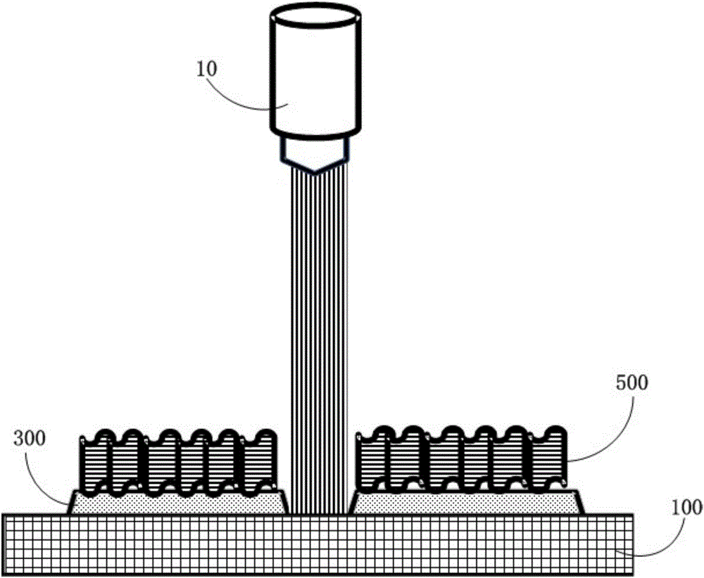
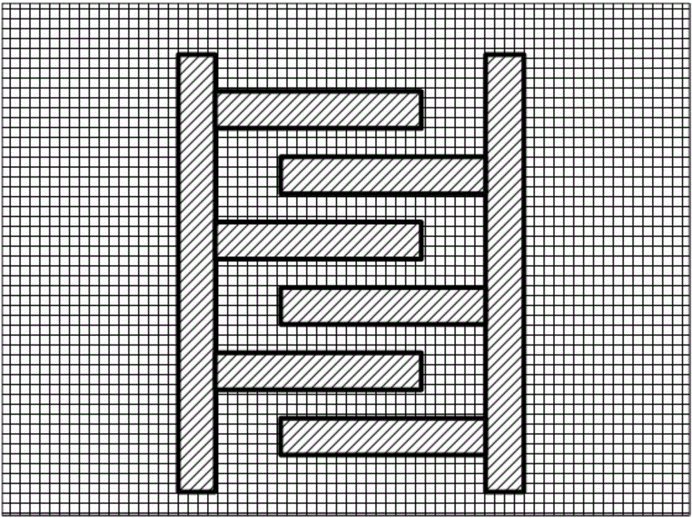
[0021] Such as figure 1 As shown, the preparation method of the planar energy storage device in this specific embodiment includes the following steps:
[0022] S1. Select an insulating substrate, and form a uniform conductive layer on the insulating substrate by means of magnetron sputtering, chemical plating, vacuum evaporation or coating.
[0023] In this step, the insulating base can be selected from polyethylene terephthalate (PET) film, polyethylene naphthalate (PEN) film, polyvinyl chloride film, polyimide (PI) film, ring Oxygen resin substrate, resin glass fiber board, medium temperature co-fired ceramic chip (MLCC), glass and other materials. The formation of the conductive layer can be accomplished by magnetron sputtering, vacuum evaporation, electroless plating or coating techniques.
[0024] Specifically, the insulating substrate (length 20-1000mm, width 20-500mm, thickness 3-1000μm) is cleaned with alcohol, acetone, etc., and then dried in an oven at 60°C for 2-3...
Embodiment 1
[0038] In this embodiment, the insulating substrate is made of PET film, the material of the conductive layer is made of nickel film, the active material is made of graphene, the packaging film is made of PET film, and the hot melt adhesive is made of PU.
[0039] A flexible polyethylene terephthalate (PET) film with a thickness of 6 μm is used as a substrate, and a nickel film (Ni) with a thickness of 500 nm is plated on the surface of the substrate by magnetron sputtering technology as a current collector.
[0040] Graphene oxide (GO) was prepared by the modified Hummers method as a precursor material, and GO was fully dispersed using an ultrasonic cell pulverizer (power 240W, frequency 25kHz, ultrasonic time 2h), and then the GO dispersion was mixed with absolute ethanol by Blending and stirring at a certain volume ratio for 1-2 hours. Then, use electrostatic spraying technology to fix the PET / Ni film on the working panel, control the temperature at 20-80°C, the high voltag...
Embodiment 2
[0048] In this embodiment, the insulating substrate is made of PI film, the conductive layer material is made of carbon powder material, and the active material is made of MnO 2 , the packaging film is made of ABS film, and the hot melt adhesive is made of silicone resin.
[0049] A 20 μm thick PI film was selected as the substrate, and cleaned with alcohol and acetone before use. After drying, use the coating technology to coat the conductive carbon paste (carbon powder: bisphenol A epoxy resin: curing agent: diluent mass ratio is 41:5:3:1) on the surface of the substrate, and control the coating machine Parameters: film thickness: 30μm, coating speed: 1cm / s, curing temperature: 140°C, so as to obtain a uniform conductive carbon paste current collector.
[0050] Prepare a 0.1-5M potassium permanganate solution, mix it uniformly and use it as a deposition solution, use the above-mentioned conductive layer as an anode, and a platinum electrode as a cathode, apply a DC voltage ...
PUM
| Property | Measurement | Unit |
|---|---|---|
| thickness | aaaaa | aaaaa |
| thickness | aaaaa | aaaaa |
| width | aaaaa | aaaaa |
Abstract
Description
Claims
Application Information


