Smart Solid Low Voltage DC Electrical Junction Box
An electrical junction box, low-voltage direct current technology, applied in the direction of electrical components, conductive connections, connections, etc.
- Summary
- Abstract
- Description
- Claims
- Application Information
AI Technical Summary
Problems solved by technology
Method used
Image


Examples
specific Embodiment approach 1
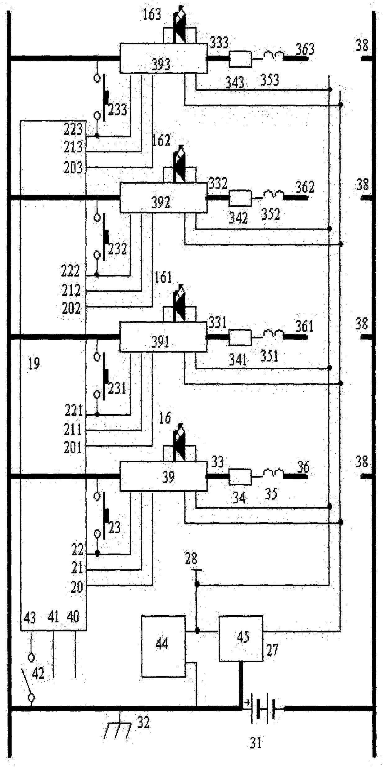
[0048] The specific circuit implementation mode 1 is a positive voltage control output type solid junction box, figure 1 is the circuit diagram of one of the branches; figure 2 It is the internal circuit diagram of the power supply regulator 29 of one of the branch MOS transistors 1 driving the IC26 in the positive voltage control output type electrical junction box; image 3 It is a circuit wiring schematic diagram of using one CPU 19 to control the positive voltage control output of 4 branches; the CPU 19 adopts Hongjing STC15F2K series or other single-chip microcomputers that meet the functional requirements.
[0049] In this embodiment, the main switching power element of each power supply branch adopts N-channel MOS transistor 1, and each branch N-channel MOS transistor can be one, or multiple can be connected in parallel as a power supply output branch. The drains of the main switch N-channel MOS transistors 1 of all solid junction boxes are connected to the positive e...
specific Embodiment approach 2
[0063] The specific circuit implementation mode 2 is a negative voltage control output type solid junction box, Image 6 is the circuit diagram of one of the branches, Figure 4 It is a circuit wiring schematic diagram of using 1 CPU 19 to control 4 branch negative voltage control outputs.
[0064] Only the differences from the circuit hardware embodiment 1 will be described below
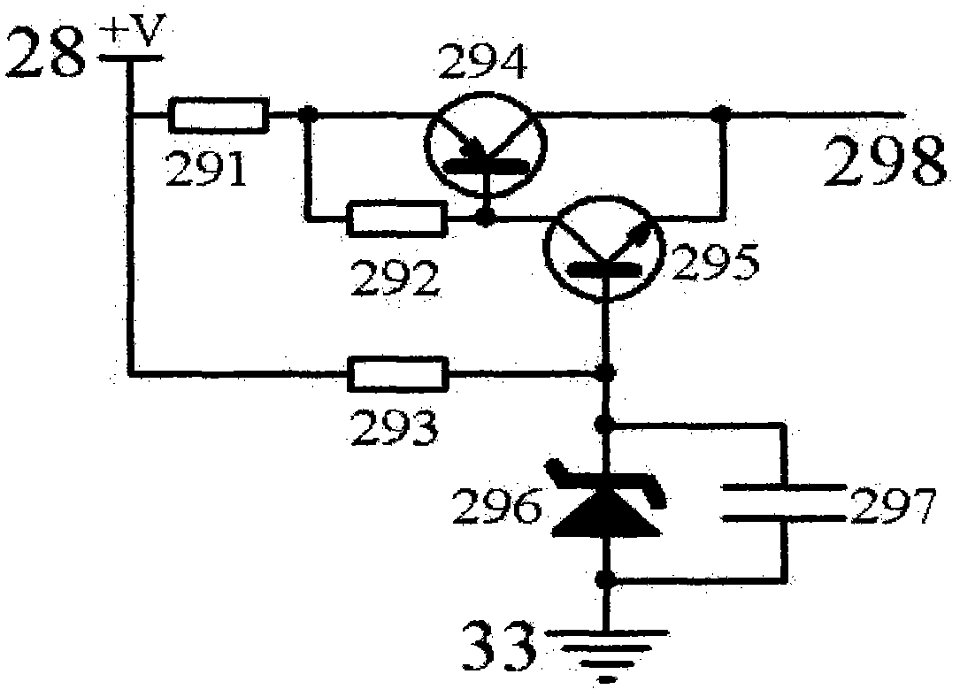
[0065] Image 6 Among them, the sampling resistance of the output current is still replaced by the channel resistance when the main switch N-channel MOS transistor of this branch is turned on, and the current sampling signal of the current sampling point 33 is sent to the non-inverting input terminal of the amplifier 4 through the current limiting resistance 37, and the current The inverting input terminal of the sampling signal amplifier 4 is connected in series with the compensation thermistor 3 through the resistor 2 and then grounded; the common ground terminal of all amplification, compariso...
PUM
 Abstract
Description
Claims
Application Information
 - R&D
- Intellectual Property
- Life Sciences
- Materials
- Tech Scout
- Unparalleled Data Quality
- Higher Quality Content
- 60% Fewer Hallucinations
Browse by: Latest US Patents, China's latest patents, Technical Efficacy Thesaurus, Application Domain, Technology Topic, Popular Technical Reports.
© 2025 PatSnap. All rights reserved.Legal|Privacy policy|Modern Slavery Act Transparency Statement|Sitemap|About US| Contact US: help@patsnap.com