
Passivation method of semiconductor device and semiconductor device

A semiconductor and device technology, applied in the field of semiconductor devices, can solve problems such as catastrophic failure and electrical characteristic degradation

Inactive Publication Date: 2016-09-21
SICHUAN HONGXINWEI TECH
View PDF8 Cites 1 Cited by
  • Summary
  • Abstract
  • Description
  • Claims
  • Application Information

AI Technical Summary

Problems solved by technology

Under BT-stress conditions, such as: under high temperature and strong electric field conditions formed by reverse voltage, sodium ions eventually gather near the reverse-biased electrode region of the semiconductor device, creating a conductive channel on the device surface, which will lead to The degradation of electrical characteristics can even lead to catastrophic failure

Method used


Image

  • Passivation method of semiconductor device and semiconductor device
  • Passivation method of semiconductor device and semiconductor device

Examples


Embodiment Construction

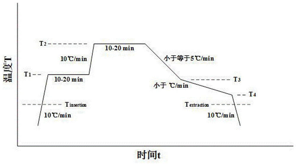
[0019] figure 1 It is the temperature-time curve diagram of typical glass passivation layer formation in the prior art, for example: the patent CN1183582C of the People's Republic of China on January 5, 2005, for a specific glass component, the DTA melting curve of glass. It can be seen that from the temperature T after the melting (glass forming) step 2 To the starting point temperature T of the annealing step 3 , the cooling rate (temperature-time gradient) is 5°C / min, the cooling rate of the annealing step is 2˚C / min, followed by the end point temperature T of the annealing step 4 To the end point temperature T of the annealing step 4 Below 25°C, the cooling rate is converted to about 10°C / min.

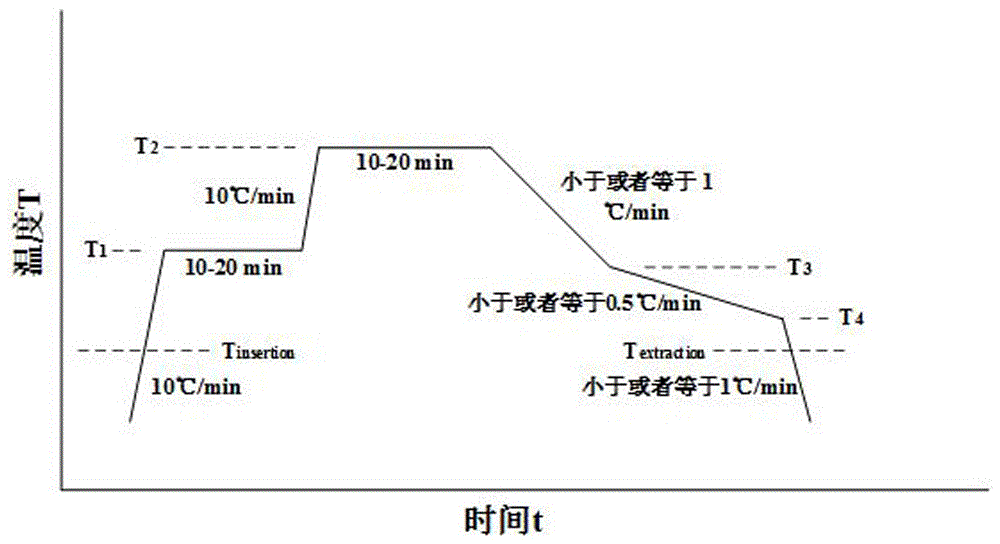
[0020] Regarding the formation of lead oxide silicate passivated glass, the specific implementation of this proposal is as follows: In the glass melting step (in an atmosphere of nitrogen or nitrogen and oxygen at 820˚C, 15-30 minutes) T 2 The subsequent cooling rate is 1°C / min...


PUM


Abstract

The invention provides a passivation method of a semiconductor device. The passivation method comprises a forming process, for example, a deposition stage, a vitrification stage, a melting stage, an annealing stage and a cooling stage. In order to improve the reliability of the semiconductor device under a high-temperature reverse bias, silicate oxide glass protection layers are different. In order to reduce the strain, the cooling rate after melting is less than or equal to 1 DEG C / min from at least 10-15 DEG C below the temperature of an annealing starting point; and at the annealing stage, the cooling rate should be less than or equal to 0.5 DEG C / min.

Description

technical field [0001] The invention relates to a semiconductor device, especially a surface passivation device mainly using silicate, such as plumbous oxide or zinc oxide-aluminosilicate. Oxide glass protective layers are suitable for high-voltage applications, and more specifically, it involves high-reliability devices, especially under high bias temperature stress (BT-stress) conditions. Background technique [0002] Due to the high sensitivity of device parameters to contamination and accumulation of mobile charges near the P-N junction, surface passivation of semiconductor devices is considered to be one of the main factors to achieve high reliability in demanding applications. Among the various designs and methods of passivation, the known glass passivation prior art, for example: US Patent 3212921 published on October 19, 1965 or Chinese patent CN1183582C published on January 5, 2005, is based on chemical It is well known to provide good passivation coatings for semi...

Claims


Application Information

Patent Timeline
IPC IPC(8): H01L21/02
CPCH01L21/02255
Inventor 李学良西里奥·艾·珀里亚科夫
Owner SICHUAN HONGXINWEI TECH
Learn More