AlGaInP-based light emitting diode wafer with high brightness and reversed polarity, and manufacturing method thereof

A technology of light-emitting diodes and manufacturing methods, applied in electrical components, circuits, semiconductor devices, etc., can solve the problems of reducing product yield, identification difficulty, and product competitiveness, etc., and achieve luminous efficiency and product yield. the effect of improving the competitiveness of products

Active Publication Date: 2016-09-21
YANGZHOU CHANGELIGHT
View PDF4 Cites 8 Cited by
  • Summary
  • Abstract
  • Description
  • Claims
  • Application Information

AI Technical Summary

Problems solved by technology

[0004] In the traditional wafer production process, in order to make the ITO thin film layer and the p-GaP window layer form a good electrical contact, it is necessary to make a dielectric film conductive hole layer that is uniformly distributed between the ITO thin film layer and the p-GaP window layer. Some conductive holes will inevitably appear on the cutting track. After the back-end cutting, the black color of the holes will make it difficult for the visual inspection machine to identify the core particles. Yield
When the client is performing die bonding operations, it will also cause difficult identific

Method used


Image

  • AlGaInP-based light emitting diode wafer with high brightness and reversed polarity, and manufacturing method thereof
  • AlGaInP-based light emitting diode wafer with high brightness and reversed polarity, and manufacturing method thereof
  • AlGaInP-based light emitting diode wafer with high brightness and reversed polarity, and manufacturing method thereof

Examples


Embodiment Construction

[0029] 1. Manufacturing process steps:

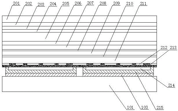
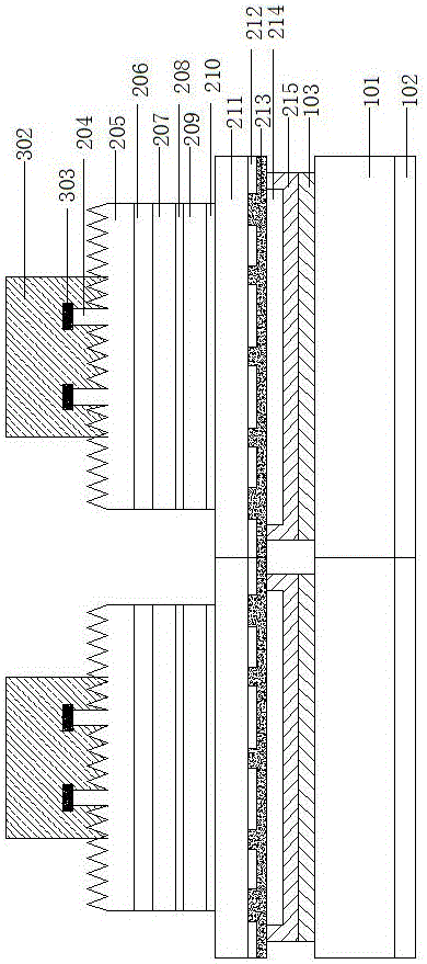
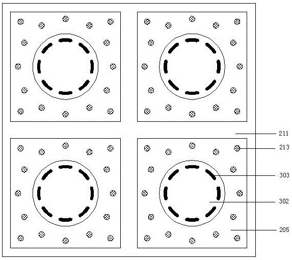
[0030] 1. If figure 1 As shown, an epitaxial layer is grown on a GaAs temporary substrate 201 by MOCVD equipment, and the epitaxial layer includes a transition layer 202, an N-GaInP cut-off layer 203, an N-GaAs ohmic contact layer 204, an N-AlGaInP roughening layer 205, and an N-AlGaInP Current spreading layer 206 , N-AlGaInP confinement layer 207 , MQW multi-quantum well active layer 208 , P-AlGaInP confinement layer 209 , buffer layer 210 , and P-GaP window layer 211 .

[0031] Wherein the thickness of the N-GaAs ohmic contact layer 204 is 35-50nm (preferably 40nm), the doping element is Si, and the doping concentration is 1×10 19 cm -3 Above, to ensure that the N surface has a good current spreading ability; the thickness of the N-AlGaInP current spreading layer 206 is 2000nm; the thickness of the P-GaP window layer 211 is 1500-3000nm (preferably 2000nm), the doping element is Mg, doped Concentration at 1×10 18 cm -3 Above, to e...


PUM

PropertyMeasurementUnit
Thicknessaaaaaaaaaa
Thicknessaaaaaaaaaa
Thicknessaaaaaaaaaa

Abstract

The invention provides an AlGaInP-based light emitting diode wafer with high brightness and reversed polarity, and a manufacturing method thereof, and relates to the technical field of manufacturing an AlGaInP (quaternary system) light emitting diode. The manufacturing method of the AlGaInP-based light emitting diode wafer includes the steps: taking one crystal grain as one unit, manufacturing distributed reflector layers on an ITO film layer, and respectively manufacturing a first metal bonding layer in a wrapping mode on each reflector layer; and taking one crystal grain as one unit, manufacturing distributed a second metal bonding layer on a permanent substrate. The manufacturing method of the AlGaInP-based light emitting diode wafer is simple and reasonable in the technology, and only changes the manufacturing process of the distributed reflector layer, the first metal bonding layer and the second metal bonding layer to enable the bonded semi-finished product to form intervals between the adjacent crystal grains so as to be conductive to the subsequent process of segmenting the whole wafer into independent crystal grains to effectively improve the luminescence efficiency and the product yield rate of the finished diode.

Description

technical field [0001] The invention belongs to the technical field of optoelectronics, in particular to the technical field of manufacturing AlGaInP quaternary light-emitting diodes. Background technique [0002] Quaternary AlGaInP is a semiconductor material with direct wide bandgap, which has been widely used in the preparation of various optoelectronic devices. Since the light-emitting band of the material can cover the 390-780nm band of visible light, more and more attention has been paid to the visible light high-brightness light-emitting diodes made of this material. Light-emitting diodes, especially AlGaInP (quaternary system) red high-brightness light-emitting diodes, have been widely used in many aspects such as outdoor display, monitoring lighting, and car lights. [0003] Compared with AlGaInP LED chips with ordinary structures, high-brightness AlGaInP chips realize substrate replacement through bonding technology, and use silicon substrates with good thermal co...

Claims


Application Information

Patent Timeline
IPC IPC(8): H01L33/38H01L33/46H01L33/00
CPCH01L33/007H01L33/38H01L33/46
Inventor 李波杨凯何胜徐洲林鸿亮张永张双翔
Owner YANGZHOU CHANGELIGHT
Why Eureka
Try Eureka