Light-emitting diode with distributed conductive hole structure and its manufacturing method

A technology of light-emitting diodes and manufacturing methods, which is applied in the direction of circuits, electrical components, semiconductor devices, etc., can solve the problems of difficult identification of chips in visual inspection machines, lower product yields, and low light extraction efficiency, so as to improve product yields and improve The pass rate and the effect of improving luminous efficiency

Active Publication Date: 2017-07-04
YANGZHOU CHANGELIGHT
View PDF5 Cites 0 Cited by
  • Summary
  • Abstract
  • Description
  • Claims
  • Application Information

AI Technical Summary

Problems solved by technology

The traditional reflective layer structure is composed of a dielectric film and a metal layer with uniform openings on the entire surface. Due to the uniform distribution of conductive holes on the P surface, the current on the P surface can flow uniformly to the active area after injection, but due to the shading effect of the N surface electrode, As a result, the current injection in the conductive hole under the electrode becomes invalid injection, resulting in low light extraction efficiency
In addition, the traditional evenly distributed conductive holes will inevitably appear on the cutting line after the back-end cutting. The black color of the holes will make it difficult for the visual inspection machine to identify the core particles, and it will also be difficult to identify the core particles during abnormal picking. Misjudgment caused by removal, reducing product yield
When the client is performing die bonding operations, it will also cause difficult identification problems, which will bring customer complaints and even affect product reputation

Method used


Image

  • Light-emitting diode with distributed conductive hole structure and its manufacturing method
  • Light-emitting diode with distributed conductive hole structure and its manufacturing method
  • Light-emitting diode with distributed conductive hole structure and its manufacturing method

Examples


Embodiment Construction

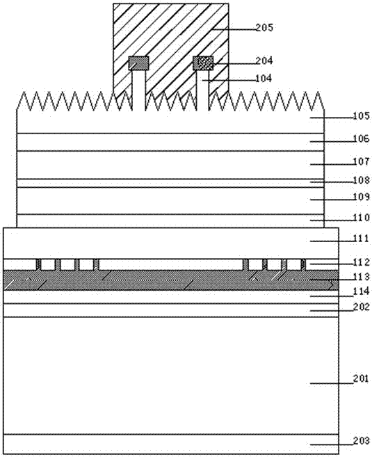
[0025] One, such as figure 1 and 2 Shown is a schematic view of the structure of a preferred example of the present invention during the manufacturing process, and the manufacturing steps are as follows:

[0026] 1. If figure 1 As shown, a transition layer 102, an N-GaInP cut-off layer 103, an N-GaAs ohmic contact layer 104, an N-AlGaInP roughening layer 105, and an N-AlGaInP current spreading layer 106 are sequentially grown on a temporary GaAs substrate 101 by MOCVD equipment. , N-AlGaInP confinement layer 107, MQW multiple quantum well active layer 108, P-AlGaInP confinement layer 109, buffer layer 110, P-GaP current spreading layer 111.

[0027] Wherein the N-GaAs ohmic contact layer 104 preferably has a thickness of 40nm and a doping concentration of 1×10 19 cm -3 Above, the doped impurity element is Si to ensure that the N surface has a good current spreading ability; the P-GaP current spreading layer 111 preferably has a thickness of 2000nm and a doping concentratio...


PUM


Abstract

A light-emitting diode with a distributed conductive hole structure and a manufacturing method thereof belong to the field of optoelectronic technology. A specular reflection layer is fabricated on an epitaxial wafer, a substrate is bonded on the specular reflection layer, and the substrate, buffer layer and cut-off layer on the epitaxial wafer are removed. Expose the N-GaAs ohmic contact layer, and then make a patterned N-GaAs ohmic contact layer, extension electrodes, main electrodes and back electrodes. In the present invention, each through hole in the SiO2 conductive hole layer and the mirror layer jointly constitute a specular reflection layer, and the AuZn in the SiO2 hole forms a good electrical contact with the P-GaP current spreading layer; A Schottky junction is formed, thereby reducing the invalid injection of current and improving the luminous efficiency.

Description

technical field [0001] The invention belongs to the technical field of optoelectronics, in particular to the technical field of manufacturing AlGaInP quaternary light-emitting diodes. Background technique [0002] Quaternary AlGaInP is a semiconductor material with direct wide bandgap, which has been widely used in the preparation of various optoelectronic devices. Since the light-emitting band of the material can cover the red to yellow-green bands of visible light, the high-brightness light-emitting diodes made of visible light have attracted extensive attention. Quaternary AlGaInP red high-brightness light-emitting diodes have been widely used in many aspects such as outdoor displays, traffic lights, and car lights. Compared with AlGaInP LED chips with ordinary structures, high-brightness AlGaInP chips use bonding technology to realize substrate replacement, and use silicon substrates with good thermal performance (the thermal conductivity of silicon is about 1.5W / K.cm) ...

Claims


Application Information

Patent Timeline
Patent Type & Authority Patents(China)
IPC IPC(8): H01L33/10
CPCH01L33/005H01L33/10H01L2933/0008
Inventor 白继锋马祥柱杨凯陈亮李俊承陈宝张银桥
Owner YANGZHOU CHANGELIGHT
Why Eureka
Try Eureka