
A preparation method for improving the reliability of semiconductor lasers

A laser and semiconductor technology, applied in the structure of the active area and other directions, can solve the problems of the disorder of the lateral light mode of the semiconductor laser, the change of the transverse mode and the longitudinal mode of the laser, etc., to achieve easy operation, improve device reliability, and a wide range of applications. Effect

Active Publication Date: 2019-03-22
Shandong Huaguang Optoelectronics Co. Ltd.
View PDF7 Cites 0 Cited by
  • Summary
  • Abstract
  • Description
  • Claims
  • Application Information

AI Technical Summary

Problems solved by technology

[0011] Some patents in the above documents only provide one of the methods for removing the gallium arsenide ohmic contact layer and the window structure of the non-implanted region other than the ridge-shaped mesa, and the method of introducing the window structure of the non-implanted region given by other patents will lead to The change of the refractive index of the shaped waveguide makes the lateral light mode of the semiconductor laser disorder, resulting in the change of the transverse mode and longitudinal mode of the laser.

Method used


Image

  • A preparation method for improving the reliability of semiconductor lasers
  • A preparation method for improving the reliability of semiconductor lasers
  • A preparation method for improving the reliability of semiconductor lasers

Examples


Embodiment 1

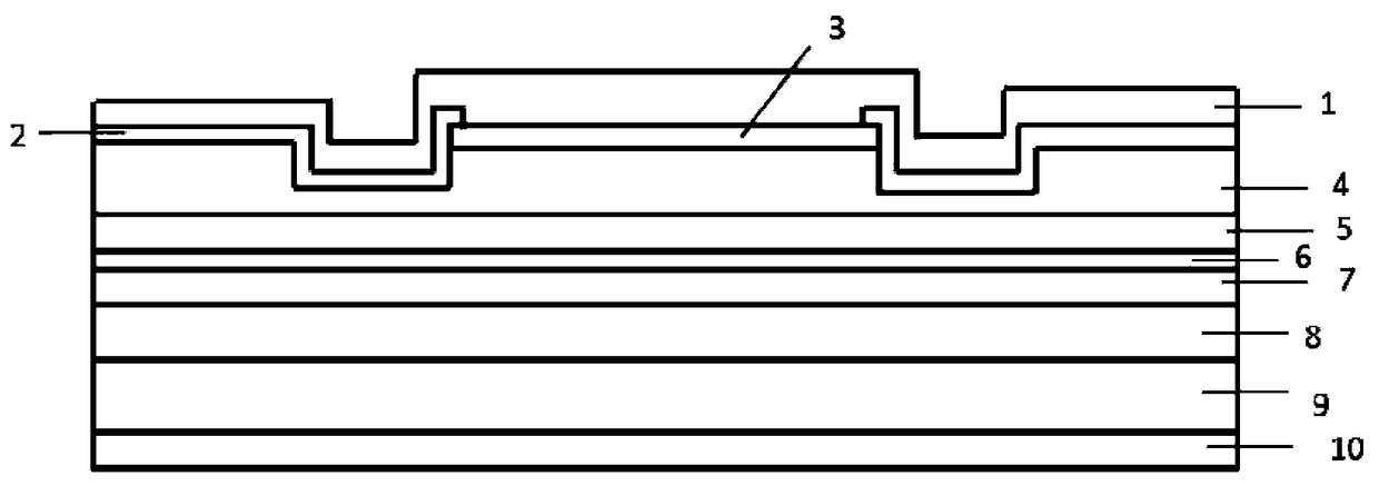
[0045] The epitaxial layer of the selected chip is a GaAs / GaInP selective etching material structure. The semiconductor laser tube core resonator has a length of 1500 μm and a width of 500 μm, a ridge waveguide width of 100 μm, and double grooves on both sides of the ridge. The double-groove ridge waveguide is fabricated by method of etching.

[0046] A preparation method for improving the reliability of a semiconductor laser, which adopts one-time etching to simultaneously remove the ohmic contact layer other than the ridge-shaped mesa of the semiconductor laser, and introduces a non-implantation region window structure; the preparation method for improving the reliability of the semiconductor laser includes specific steps as follows :

[0047] (1) On the substrate 9, grow an N-type lower confinement layer 8, a lower waveguide layer 7, an active region 6 with a quantum well structure, an upper waveguide layer 5, a P-type upper confinement layer 4, and an ohmic contact layer 3...

Embodiment 2

[0059] A kind of preparation method that improves the reliability of semiconductor laser as described in embodiment 1, its difference is that,

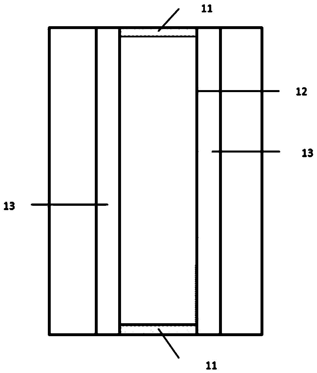
[0060] In steps (1)-(2), the window of the quantum well mixed region is prepared on the epitaxial wafer, and the active region of the window region is mixed by zinc expansion or other methods; wherein the non-implanted region window structure 11 is engraved on the quantum well In the center of the window in the cluttered area.

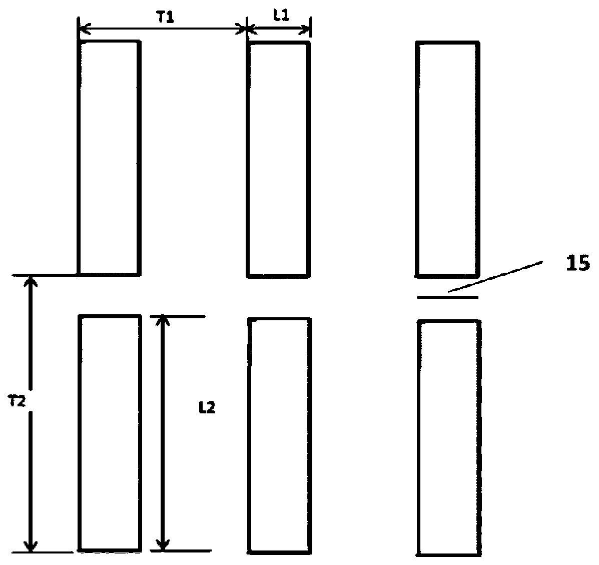
[0061] On the epitaxial wafer, a rectangular pattern arranged periodically is photo-etched, wherein the length L2 of the rectangular pattern is 1450 μm, the width L1 is 120 μm, the longitudinal period T2 is 1500 μm, and the lateral period T1 is 500 μm; the ohmic contact layer outside the rectangular pattern is removed by etching , exposing the P-type upper confinement layer, removing the ohmic contact layer other than the ridge-shaped mesa and introducing the non-implantation region window structure 11; wherei...

Embodiment 3

[0063] A preparation method for improving the reliability of a semiconductor laser as described in Example 1, the difference is that the selected chip epitaxial layer is a non-selective etching material structure of GaAs / AlGaAs, when the ohmic contact layer and the P-type The two-layer structure of the confinement layer is non-selective etching, or the ridge mesa is directly prepared by dry etching, then the size of the rectangular figure is: the width L1 of the rectangular figure ≤ the width of the ridge mesa of the semiconductor laser, the length of the rectangular figure L2 = (the resonant cavity length of the semiconductor laser chip - the width of the window structure in the non-implanted region). The length of the semiconductor laser die resonator is 2000 μm, the width is 500 μm, the width of the ridge waveguide is 200 μm, and the width of the double grooves on both sides of the ridge is 30 μm. The double groove ridge waveguide is made by wet etching method.

[0064] (1)...


PUM


Abstract

A preparation method of improving semiconductor laser reliability is characterized by removing the ohmic contact layers beyond a ridge shape mesa of a semiconductor laser simultaneously by primary etching, and introducing a non-injection region window structure. According to the present invention, based on the Schottky contact principle of a P electrode and a chip epitaxial layer, the ohmic contact layers beyond the ridge shape mesa and at a cavity surface are removed simultaneously by a primary etching process, and the non-injection region window structure is introduced, so that a Schottky contact layer is formed, and the purposes of preventing the electric leakage at the two sides of a dual-groove region in the laser and improving the reliability and a COD threshold value, are achieved. The method of the present invention only adopts a primary photoetching process, is simple in preparation technology, wide in application range and strong in compatibility, and can be combined with other special technologies, thereby improving the performances of the semiconductor laser further.

Description

technical field [0001] The invention discloses a preparation method for improving the reliability of a semiconductor laser, and belongs to the technical field of semiconductor laser manufacture. technical background [0002] Since the advent of semiconductor lasers in the 1860s, the rapid development of semiconductor lasers has attracted worldwide attention. Today, high-power semiconductor lasers have been widely used in pumping solid-state lasers, optical fiber communications, material processing, medical treatment, and laser printing due to their advantages of high efficiency, high power, and high reliability. At the same time, with the continuous expansion of new applications, the requirements for high-power semiconductor lasers are also increasing. [0003] Among them, how to achieve high power while ensuring or even improving reliability has become a key issue facing the further development of high-power semiconductor laser technology industry and market applications. ...

Claims


Application Information

Patent Timeline
Patent Type & Authority Patents(China)
IPC IPC(8): H01S5/34
Inventor 刘欢沈燕徐现刚
Owner Shandong Huaguang Optoelectronics Co. Ltd.
Learn More