Method for producing high power gallium arsenic/aluminum gallium arsenic laser non-absorption window by AlN
A laser, aluminum gallium arsenic technology, applied in the field of semiconductor optoelectronic devices, can solve the problems of low thermal conductivity and high thermal conductivity
- Summary
- Abstract
- Description
- Claims
- Application Information
AI Technical Summary
Problems solved by technology
Method used
Image
Examples
Embodiment Construction
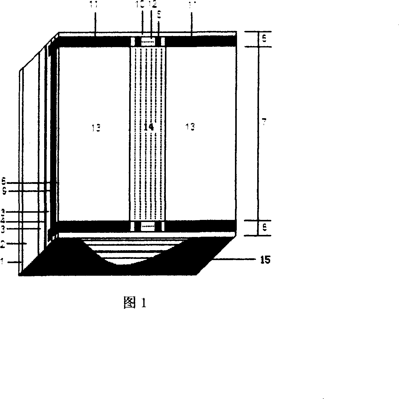
[0012] Please refer to Figure 1. The method of using AlN to make a non-absorbing window of a high-power GaAs / AlGaAs laser is: the original material is a GaAs / AlGaAs epitaxial wafer, and the epitaxial wafer includes a substrate 2 and an epitaxial layer 3 , the depth of the active region 4 from the surface is 1.7 microns; on the window region 6 and the implant region 7, use photolithography to cover the regions 10, 13 and 14 with photoresist AZ-1350, and remove the light from the regions 11 and 12. Resist; use etching solution (sulfuric acid: water: hydrogen peroxide = 9: 4: 4) to etch 0.8-1.2 microns in areas 11 and 12; use reactive magnetron sputtering method to grow on the epitaxial wafer surface at 200-300 °C 0.4-0.8 micron AlN8; use acetone to ultrasonically clean the photoresist and the AlN layer on the regions 10, 13, 14; and then use the photoresist AZ-1350 to cover the regions 10, 11, 12 and 14, remove the photoresist in area 13; use etching solution (sulfuric acid: wat...
PUM
| Property | Measurement | Unit |
|---|---|---|
| Thickness | aaaaa | aaaaa |
Abstract
Description
Claims
Application Information
