Band-gap modified Ge CMOS integrated device and manufacturing method thereof
What is AI technical title?
AI technical title is built by Patsnap AI team. It summarizes the technical point description of the patent document.
An integrated device and modified technology, which is applied in semiconductor/solid-state device manufacturing, electrical components, transistors, etc., can solve problems such as unfavorable alloy growth, and achieve the effect of simple preparation technology
Active Publication Date: 2016-10-12
XIDIAN UNIV
View PDF2 Cites 1 Cited by
Summary
Abstract
Description
Claims
Application Information
AI Technical Summary
This helps you quickly interpret patents by identifying the three key elements:
Problems solved by technology
Method used
Benefits of technology
Problems solved by technology
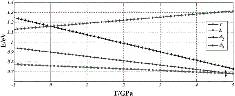
Again, the lattice mismatch between Ge and a-Sn is as high as 14.7%, which is also not conducive to Ge 1-x sn x alloy growth
Method used
Image
Click on the blue label to locate the original text in one second.
Reading with bidirectional positioning of images and text.
Examples
Embodiment 1
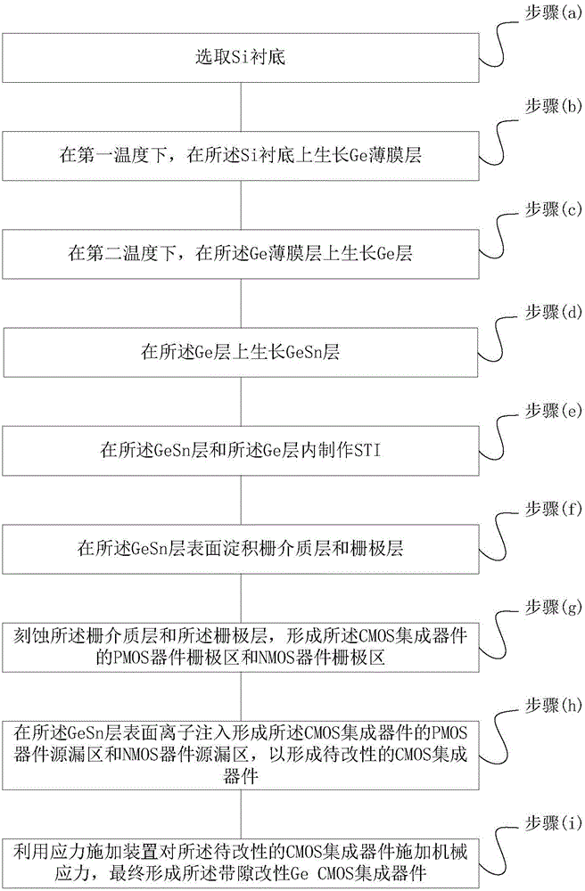
[0073] See figure 2 , figure 2 A flow chart of a method for preparing a direct bandgap Ge CMOS integrated device provided by an embodiment of the present invention; the method includes the following steps:
[0075] Step (b), at a first temperature, growing a Ge thin film layer on the Si substrate;
[0076] Step (c), at a second temperature, growing a Ge layer on the Ge thin film layer;
[0077] Step (d), growing a GeSn layer on the Ge layer;
[0078] Step (e), making STI in the GeSn layer and the Ge layer;
[0079] Step (f), depositing a gate dielectric layer and a gate layer on the surface of the GeSn layer;
[0080] Step (g), etching the gate dielectric layer and the gate layer to form a PMOS device gate region and an NMOS device gate region of the CMOS integrated device;
[0081] Step (h), ion implantation on the surface of the GeSn layer to form the source and drain regions of the PMOS device and the source and drain regio...
Embodiment 2
[0110] See Figure 4a-Figure 4u , Figure 4a-Figure 4u A schematic diagram of a method for fabricating a direct bandgap Ge CMOS integrated device provided by an embodiment of the present invention. On the basis of the above embodiments, this embodiment will introduce the process flow of the present invention in more detail. The method includes:
[0111] S101. Substrate selection. Such as Figure 4a As shown, the Si substrate sheet 201 whose crystal orientation is (001) is selected as the original material;
[0112] S102. Using the method of molecular beamepitaxy (MBE), on the Si substrate 201, grow an n-type Ge film with a crystal orientation of (001) on the Si substrate 201 by a two-step method of low temperature and high temperature, and the doping concentration is 1×10 16 ~5×10 16 cm -3 . specifically:
[0113] S1021, such as Figure 4b As shown, a 50 nm thick "low temperature" Ge ((LT-Ge) film 202 was grown at 275 ~ 325 °C. Most of the relaxation of elastic stres...
PUM
Abstract
The invention relates to a band-gap modified Ge CMOS integrated device and a manufacturing method thereof. The manufacturing method comprises the steps of: selecting an Si substrate; growing a Ge thin film layer and a Ge layer on the Si substrate; growing a GeSn layer on the Ge layer; manufacturing an STI in the GeSn layer and the Ge layer; depositing a gate dielectric layer and a gate layer on the surface of the GeSn layer; etching the gate dielectric layer and the gate layer and forming gate regions of a PMOS device and an NMOS device; and carrying out ion implantation on the surface of the GeSn layer to form a PMOS device source-drain region and an NMOS device source-drain region of the CMOS integrated device, applying mechanical stress to the to-be-modified CMOS integrated device by a stress applying device and finally forming the band-gap modified Ge CMOS integrated device. A channel material utilized by the CMOS device is a direct band-gap modified Ge material; the carrier mobility of the channel material is improved by multiple times in comparison with that of a traditional Si material; the current drive and frequency characteristics of the CMOS integrated device are improved; and the device is suitable for monolithic optoelectronic integration with a photonic device.
Description
technical field [0001] The invention relates to the technical field of integrated circuits, in particular to a bandgap modified Ge CMOS integrated device and a preparation method thereof. Background technique [0002] For many years, scaling MOSFETs has been used to increase device speed along the path provided by Moore's Law. However, with the reduction of MOSFET size, the conventional scaling method has encountered a series of problems centered on the short-channel effect. For complementary metaloxidesemiconductor (Complementary MetalOxideSemiconductor, CMOS for short) devices, how to improve carrier mobility becomes the key to maintain their performance. Although the strained Si material applied to the device can improve the carrier mobility, the effect is close to the limit. Moreover, because the hole mobility of the Si material is lower than the electron mobility, the performance of the CMOS circuit is largely restricted by the PMOS, which limits the further impro...
Claims
Application Information
Patent Timeline
Application Date:The date an application was filed.
Publication Date:The date a patent or application was officially published.
First Publication Date:The earliest publication date of a patent with the same application number.
Issue Date:Publication date of the patent grant document.
PCT Entry Date:The Entry date of PCT National Phase.
Estimated Expiry Date:The statutory expiry date of a patent right according to the Patent Law, and it is the longest term of protection that the patent right can achieve without the termination of the patent right due to other reasons(Term extension factor has been taken into account ).
Invalid Date:Actual expiry date is based on effective date or publication date of legal transaction data of invalid patent.

