Amorphous silicon thin film solar cell and manufacturing method thereof
A technology for solar cells and amorphous silicon thin films, applied in the field of solar energy development, can solve the problems of high production cost, reduced service life of solar cells, and high cost, and achieves improvement of open circuit voltage and filling factor, improvement of cell conversion efficiency, and mature manufacturing process. Effect
- Summary
- Abstract
- Description
- Claims
- Application Information
AI Technical Summary
Problems solved by technology
Method used
Image
Examples
Embodiment 1
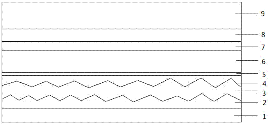
[0029] A kind of amorphous silicon thin film solar cell, its structure is as follows figure 1 As shown, the flexible PET substrate layer, SiO 2 Light trapping layer, first electrode TCO layer, p-type amorphous silicon layer, p-type buffer layer, i-type amorphous silicon layer, n-type amorphous silicon layer, second electrode TCO layer and back reflection layer; the flexible PET The thickness of the substrate layer is 0.028mm, SiO 2 The thickness of the light-trapping layer is 500nm, the thickness of the TCO layer of the first electrode is 500nm, the thickness of the TCO layer of the second electrode is 84nm, the thickness of the p-type amorphous silicon layer is 25nm, the thickness of the p-type buffer layer is 15nm, and the thickness of the i-type amorphous silicon layer The thickness of the n-type amorphous silicon layer is 17nm, and the thickness of the back reflection layer is 310nm.
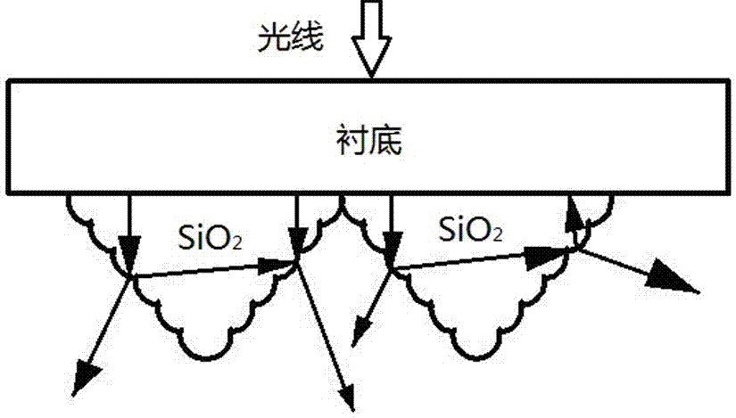
[0030] figure 2 SiO of the present invention is provided 2 Schematic diagram of the...
Embodiment 2
[0043] A kind of amorphous silicon thin film solar cell, its structure is as follows figure 1 As shown, the flexible PET substrate layer, SiO 2 Light trapping layer, first electrode TCO layer, p-type amorphous silicon layer, p-type buffer layer, i-type amorphous silicon layer, n-type amorphous silicon layer, second electrode TCO layer and back reflection layer; the flexible PET The thickness of the substrate layer is 0.018mm, SiO 2 The thickness of the light-trapping layer is 500nm, the thickness of the TCO layer of the first electrode is 500nm, the thickness of the TCO layer of the second electrode is 83nm, the thickness of the p-type amorphous silicon layer is 17nm, the thickness of the p-type buffer layer is 10nm, and the thickness of the i-type amorphous silicon layer The thickness of the n-type amorphous silicon layer is 15nm, and the thickness of the back reflection layer is 325nm.
[0044] The TCO layer of the first electrode and the TCO layer of the second electrode ...
Embodiment 3
[0056] A kind of amorphous silicon thin film solar cell, its structure is as follows figure 1 As shown, the flexible PET substrate layer, SiO 2 Light trapping layer, first electrode TCO layer, p-type amorphous silicon layer, p-type buffer layer, i-type amorphous silicon layer, n-type amorphous silicon layer, second electrode TCO layer and back reflection layer; the flexible PET The thickness of the substrate layer is 0.032mm, SiO 2 The thickness of the light-trapping layer is 400nm, the thickness of the TCO layer of the first electrode is 500nm, the thickness of the TCO layer of the second electrode is 87nm, the thickness of the p-type amorphous silicon layer is 20nm, the thickness of the p-type buffer layer is 7nm, and the thickness of the i-type amorphous silicon layer The thickness of the n-type amorphous silicon layer is 20nm, and the thickness of the back reflection layer is 326nm.
[0057] The TCO layer of the first electrode and the TCO layer of the second electrode a...
PUM
| Property | Measurement | Unit |
|---|---|---|
| thickness | aaaaa | aaaaa |
| thickness | aaaaa | aaaaa |
| thickness | aaaaa | aaaaa |
Abstract
Description
Claims
Application Information


