Graphene/carbon nanotube film Schottky junction photodetector and preparation method thereof

A carbon nanotube film and photodetector technology, which is applied in circuits, electrical components, semiconductor devices, etc., can solve the problems of low responsivity of graphene detectors, difficult collection of photogenerated carriers, and short lifetime of photogenerated carriers. , to achieve the effect of both practicability, enhanced optoelectronic properties, and fast response speed

Active Publication Date: 2017-05-17
HEFEI UNIV OF TECH
View PDF2 Cites 0 Cited by
  • Summary
  • Abstract
  • Description
  • Claims
  • Application Information

AI Technical Summary

Problems solved by technology

In the field of photoelectric detection, although graphene has a wide absorption bandwidth, there are also obvious disadvantages; intrinsic graphene itself has low light absorption rate and lack of light gain mechanism, resulting in low responsivity of graphene detectors; graphite The photogenerated carrier life of graphene itself is short, only about picoseconds, which makes it difficult to collect photogenerated carriers effectively and seriously affects the responsivity of the detector. Therefore, pure graphene-based detectors cannot meet the needs of practical applications.

Method used


Image

  • Graphene/carbon nanotube film Schottky junction photodetector and preparation method thereof
  • Graphene/carbon nanotube film Schottky junction photodetector and preparation method thereof
  • Graphene/carbon nanotube film Schottky junction photodetector and preparation method thereof

Examples


Embodiment 1

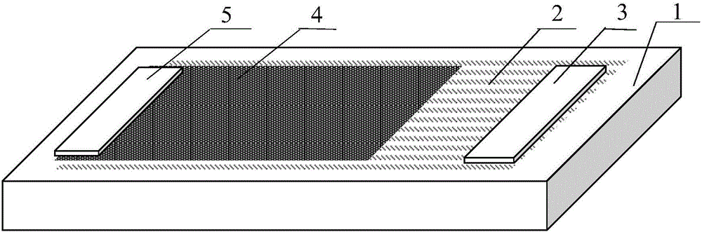
[0033] see figure 1 , the graphene / carbon nanotube film Schottky junction photodetector of the present embodiment has the following structure:

[0034] The upper surface of the insulating substrate 1 is covered with a carbon nanotube film 2, one end of the upper surface of the carbon nanotube film 2 is provided with a first silver electrode 3 that is in ohmic contact with the carbon nanotube film 2, and the other end is provided with a silver electrode 3 connected to the carbon nanotube film 2. The film 2 is a graphene film 4 in Schottky contact, and a second silver electrode 5 in ohmic contact with the graphene film is arranged on the graphene film 4 .

[0035] The graphene / carbon nanotube film Schottky junction photodetector of the present embodiment is prepared according to the following steps:

[0036] (1) Sonicate the silicon dioxide wafer with acetone, alcohol, and deionized water for 10 minutes in sequence, and then dry it with a nitrogen gun to obtain an insulating su...


PUM

PropertyMeasurementUnit
thicknessaaaaaaaaaa
thicknessaaaaaaaaaa
absorption coefficientaaaaaaaaaa

Abstract

The invention discloses a graphene / carbon nanotube thin film schottky junction photoelectric detector and a preparation method therefor. The upper surface of an insulating substrate is covered with a carbon nanotube thin film; a silver electrode which is in ohmic contact with the carbon nanotube thin film is arranged at one end of the carbon nanotube thin film while a graphene thin film which is in schottky contact with the carbon nanotube thin film is arranged at the other end of the carbon nanotube thin film; and a second silver electrode which is in ohmic contact with the graphene thin film is arranged on the graphene thin film. The photoelectric detector provided by the invention takes advantage of the broadband spectral absorption characteristic of the carbon nanotube, and is combined with the excellent characteristics of high light transmittance, low resistivity and the like of the graphene, so that detection on the light of 300-1,050nm is realized, and quite high responsivity and response speed are achieved as well; the preparation method is simple; the photoelectric detector is suitable for large-scale production; the broadband-spectrum, high-detectivity and high-response-speed photoelectric detector can be prepared; and a new prospect is explored for the full-carbon-structured photoelectric detection application.

Description

technical field [0001] The invention belongs to the field of semiconductor photoelectric detection, and in particular relates to a graphene / carbon nanotube film Schottky junction photodetector and a preparation method thereof. Background technique [0002] Electromagnetic waves are oscillating particle waves that are diffracted and emitted in space by electric and magnetic fields that are in phase and perpendicular to each other. They are electromagnetic fields that propagate in the form of waves and have wave-particle duality. The light visible to the human eye is an electromagnetic wave with a wavelength in the range of 390-760nm. Generally, the range of photoelectric detection is the ultraviolet-visible-near-infrared band. It is widely used in various fields of military and national economy. For example, it is mainly used in optical communication, flaw detection and optical instruments in the ultraviolet band, and it is mainly used in ray measurement and detection, indust...

Claims


Application Information

Patent Timeline
Patent Type & Authority Patents(China)
IPC IPC(8): H01L31/108H01L31/0256H01L31/18
CPCH01L31/0256H01L31/108H01L31/1876Y02P70/50
Inventor 罗林保张腾飞汪丹丹邹宜峰梁凤霞
Owner HEFEI UNIV OF TECH
Why Eureka
Try Eureka