

Heterojunction solar cell and preparation method thereof
A solar cell and heterojunction technology, applied in the field of solar cells, can solve problems such as lowering the conversion efficiency of solar cells, being susceptible to the effects of the external environment, and reducing the performance of solar cells, so as to save collector materials, reduce material costs, and improve The effect of the fill factor
Image

Examples
preparation example Construction
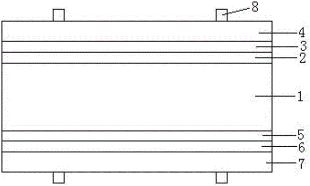
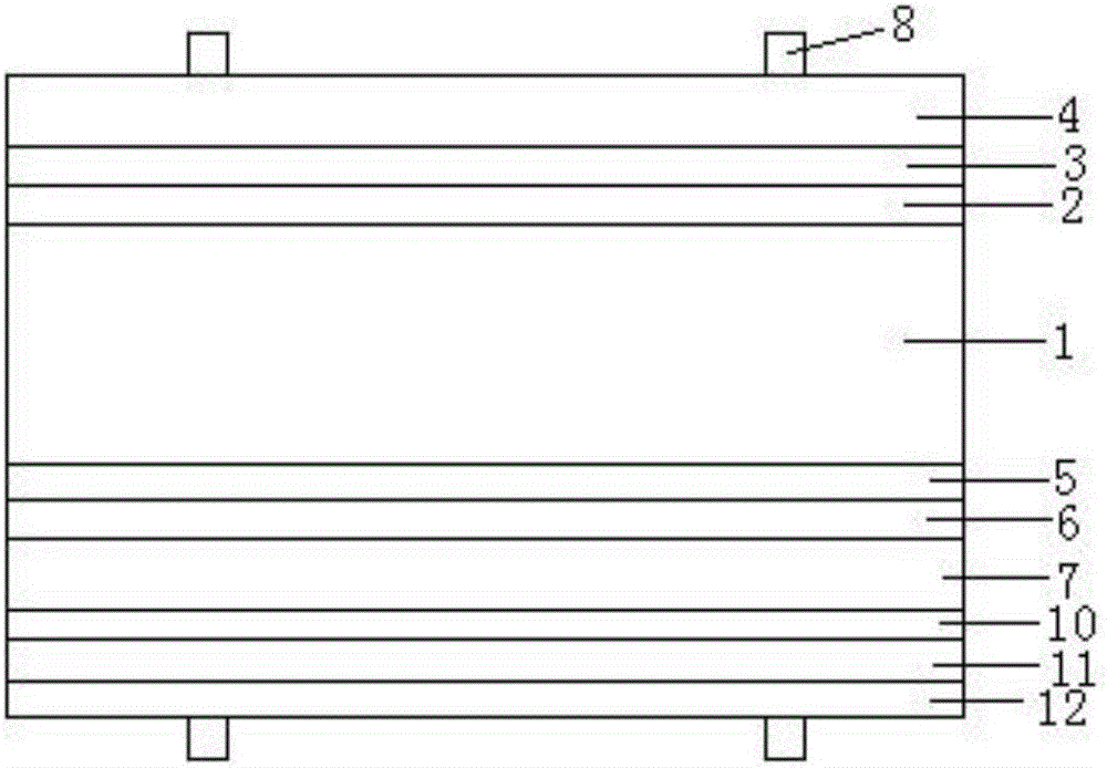
[0051] The preparation method includes: preparing a substrate 1; depositing a first intrinsic amorphous layer 2 on the light-receiving surface of the substrate 1; depositing a second intrinsic amorphous layer 5 on the back of the substrate 1; A first doped layer 3 is deposited on the first intrinsic amorphous layer 2; a second doped layer 6 is deposited on the second intrinsic amorphous layer 5; a first doped layer is deposited on the first doped layer 3. A transparent conductive layer 4; depositing a second transparent conductive layer 7 on the second doped layer 6; depositing a laminated structure on the second transparent conductive layer 7, the laminated structure includes sequentially laminated first A metal nitride film layer 10, a metal film layer 11 and a second metal nitride film layer 12, the first metal nitride film layer 10 is in direct contact with the second transparent conductive layer 7, between the first transparent conductive layer 4 and The second metal nitr...
Embodiment 1
[0056] Prepare an N-type monocrystalline silicon wafer 1 with a thickness of 200um, and then sequentially deposit 10nm intrinsic amorphous silicon film layers on the light-receiving surface of the N-type monocrystalline silicon wafer 1 as the first intrinsic amorphous layer 2 and A 25nm p-type amorphous silicon film layer is used as the first doped layer 3; then a 10nm intrinsic amorphous silicon film layer is sequentially deposited on the back of the n-type single crystal silicon wafer 1 by PECVD method as the second intrinsic amorphous silicon film layer. The n-type amorphous silicon film layer of layer 5 and 40nm is used as the second doped layer 6; Then adopts the magnetron sputtering method to deposit the ITO film layer of 100nm on the p-type amorphous silicon film layer 3 as the first transparent conductive layer 4 , then adopt magnetron sputtering method to deposit 100nm ITO film layer on n-type amorphous silicon film layer 6 as the second transparent conductive layer 7;...
Embodiment 2
[0058] Prepare an N-type monocrystalline silicon wafer 1 with a thickness of 120 μm, and then sequentially deposit 10 nm intrinsic amorphous silicon film layers on the light-receiving surface of the N-type monocrystalline silicon wafer 1 as the first intrinsic amorphous layer 2 and A 20nm p-type amorphous silicon film layer is used as the first doped layer 3; then a 10nm intrinsic amorphous silicon film layer is sequentially deposited on the back of the n-type single crystal silicon wafer 1 by PECVD method as the second intrinsic amorphous silicon film layer. The n-type amorphous silicon film layer of layer 5 and 35nm is used as the second doped layer 6; then adopts the magnetron sputtering method to deposit the ITO film layer of 100nm on the p-type amorphous silicon film layer 3 as the first transparent conductive layer 4 , then adopt magnetron sputtering method to deposit 80nm ITO film layer on n-type amorphous silicon film layer 6 as the second transparent conductive layer 7...
PUM
| Property | Measurement | Unit |
|---|---|---|
| thickness | aaaaa | aaaaa |
| thickness | aaaaa | aaaaa |
| thickness | aaaaa | aaaaa |
Abstract
Description
Claims
Application Information
- IPC
- H01L31/02; H01L31/0216; H01L31/0232; H01L31/076; H01L31/20
- CPC
- H01L31/02008; H01L31/02167; H01L31/02327; H01L31/076; H01L31/202; Y02E10/548; Y02P70/50
- Inventors
- 李艺明; 邓国云