

A high-efficiency crystalline silicon solar cell
A technology of solar cells and crystalline silicon, applied in the field of solar cells, can solve problems affecting cell efficiency, Auger recombination, etc., and achieve the effect of simple and easy preparation method, simple structure and low preparation cost
- Summary
- Abstract
- Description
- Claims
- Application Information
AI Technical Summary
Problems solved by technology
Method used
Image

Examples
Embodiment 1
[0030] This embodiment discloses a crystalline silicon solar cell with simple and effective control of Auger recombination. The cell has a simple structure and low manufacturing cost, and the conventional solar cell production line can be easily upgraded to complete the cell preparation.
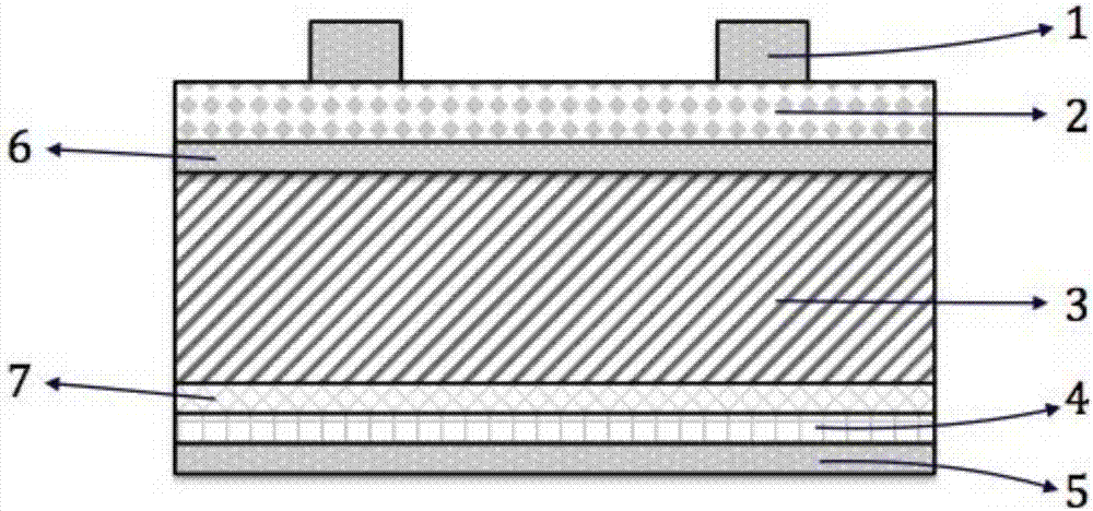
[0031] Specifically, high-efficiency crystalline silicon solar cells such as figure 1 As shown, it includes an upper electrode 1, a passivation anti-reflection SiN layer 2, a phosphorus diffusion layer 6, a base crystal silicon wafer 3, an aluminum diffusion layer 7, an adjustment layer 4 and a lower electrode 5 stacked in sequence;
[0032] The base crystalline silicon wafer 3 used in this embodiment is a p-type silicon wafer with a resistivity of 1-20Ωcm, the upper electrode is a silver electrode, and the lower electrode is an aluminum electrode. The adjustment layer 4 includes but not limited to: (1) Al 2 o 3 , SiN, SiO 2 , SiON or a composite film of their combination; (2) in order to...
Embodiment 2
[0042] This embodiment discloses a simple and effective controlled Auger recombination crystalline silicon solar cell. The cell has a simple structure and low manufacturing cost, and the cell can be manufactured by simply upgrading the traditional solar cell production line.
[0043] Specifically, a high-efficiency crystalline silicon solar cell includes an upper electrode 1, a passivation anti-reflection SiN layer 2, a phosphorus diffusion layer 6, a base crystal silicon wafer 3, an aluminum diffusion layer 7, an adjustment layer 4 and a lower electrode 5 stacked in sequence;
[0044] The base crystalline silicon wafer 3 used in this embodiment is an n-type silicon wafer with a resistivity of 1-20Ωcm, the upper electrode is a silver electrode, and the lower electrode is an aluminum electrode. Adjustment layer 4 includes but not limited to: (1) Al 2 o 3 , SiN, SiO 2 , SiON or a composite film of their combination; (2) in order to enhance the conductivity, the adjustment laye...
Embodiment 3
[0055] This embodiment discloses a method for preparing a high-efficiency crystalline silicon solar cell, which includes the following steps:
[0056] 1. Select a 2Ω·cm p-type silicon wafer, remove the damaged layer on the surface of the silicon wafer, and use KOH / IPA for surface texturing;
[0057] 2. Use phosphorus oxychloride to diffuse phosphorus on one side of the silicon wafer to form an n-type phosphorus diffusion layer on the front surface. The diffusion method is back-to-back diffusion, and the rear resistance of the expansion is 50±10Ω / □;
[0058] 3. Use the chain wet etching method to polish the back of the silicon wafer and remove the PSG, so as to remove the slight phosphorus diffusion layer on the back of the phosphorus diffusion to avoid leakage;
[0059] 4. Clean and deposit a SiN passivation anti-reflection layer on the front side;
[0060] 5. Deposit Al on the back side by ALD method 2 o 3 / ZnO quantum well material, here it is the adjustment layer with co...
PUM
| Property | Measurement | Unit |
|---|---|---|
| thickness | aaaaa | aaaaa |
| thickness | aaaaa | aaaaa |
Abstract
Description
Claims
Application Information