Sputtering deposition method of flexible AZO transparent conductive film at room temperature

A transparent conductive film, sputtering deposition technology, applied in sputtering plating, ion implantation plating, metal material coating process and other directions, can solve the problems of low optical area transmittance, small grain size, easy deformation and so on , to achieve the effect of simple process operation, good crystallization performance, compact and smooth surface

Inactive Publication Date: 2016-11-16
HENAN ANCAI HI-TECH
View PDF0 Cites 6 Cited by
  • Summary
  • Abstract
  • Description
  • Claims
  • Application Information

AI Technical Summary

Problems solved by technology

In order to obtain AZO thin films with better photoelectric properties, it is often necessary to heat flexible substrates when depositing AZO thin films by magnetron sputtering. It is easy to deform when sputtering, and organic molecules are prone to crack and pollute AZO films during sputtering, which brings certain difficulties to the preparation of flexible AZO films.
On the other hand, if the substrate temperature is too low, the crystallization quality of the AZO film will be poor, the grain size will be small, the carrier mobility will be reduced, the resistivity will be too high, and the transmittance in the visible light region will be low.

Method used


Image

  • Sputtering deposition method of flexible AZO transparent conductive film at room temperature
  • Sputtering deposition method of flexible AZO transparent conductive film at room temperature
  • Sputtering deposition method of flexible AZO transparent conductive film at room temperature

Examples


Embodiment 1

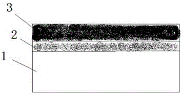
[0017] A polycarbonate (PC) film with a thickness of 0.3 mm was selected as the substrate, and the substrate was ultrasonically cleaned with acetone and absolute ethanol for 20 min, and deionized water for 15 min, and then dried and placed on the substrate holder , and the movable baffle is placed between the substrate and the target; the homogeneous buffer layer and the main layer are made of AZO ceramics with a mass ratio of aluminum oxide to zinc oxide of 2:98 as the target material, and the mechanical pump and molecular Pump vacuum to 5×10 -3 Pa, then fill the working gas with high-purity argon (99.99%) until the pressure of the vacuum chamber is 0.5 Pa, turn on the DC power supply for pre-sputtering for 15 minutes; open the movable baffle, and deposit AZO homogeneous buffer layer by DC magnetron sputtering, The sputtering conditions were as follows: sputtering power was 80 W, working pressure was 0.5 Pa, target base distance was 12 cm, substrate temperature was room temp...

Embodiment 2

[0019] A PC film with a thickness of 0.3 mm was selected as the substrate, and the substrate was ultrasonically cleaned with acetone and absolute ethanol for 20 min, and then with deionized water for 15 min. The plate is placed between the substrate and the target material; the homogeneous buffer layer and the main body layer use AZO ceramics with a mass ratio of aluminum oxide to zinc oxide of 2:98 as the target material, and turn on the mechanical pump and the molecular pump to evacuate to 5 ×10 -3 Pa, then fill the working gas with high-purity argon (99.99%) until the vacuum chamber pressure is 0.5 Pa, turn on the DC power supply for pre-sputtering for 15 minutes; open the movable baffle, and deposit AZO homogeneous buffer layer by DC magnetron sputtering, The sputtering conditions were as follows: sputtering power was 80 W, working pressure was 0.5 Pa, target base distance was 12 cm, substrate temperature was room temperature, sputtering time was 5 min, and the movable ba...


PUM

PropertyMeasurementUnit
thicknessaaaaaaaaaa
thicknessaaaaaaaaaa
electrical resistivityaaaaaaaaaa

Abstract

The invention relates to a sputtering deposition method of a flexible AZO transparent conductive film at room temperature. The method comprises the following steps of (1) cleaning a substrate; (2) presputtering; (3) preparing a homogeneous buffer layer; (4) assisting to sputter a main body layer of the AZO film by ultraviolet light. According to the sputtering deposition method, the homogeneous buffer layer which is sputtered with low power at room temperature is introduced, so that the subsequent preparation of the high-quality main body layer of the AZO film is facilitated, and damages of sputtered particles to the organic flexible substrate are reduced. The AZO film prepared by utilizing the sputtering deposition method has the advantages of good crystallization performance, compact and smooth surface and simplicity in technological operation and is suitable for industrial production.

Description

technical field [0001] The invention relates to a method for sputtering and depositing a flexible AZO transparent conductive film at room temperature, and belongs to the technical field of electronic materials. Background technique [0002] Transparent conductive oxide (TCO) thin film is an important optoelectronic material, which is widely used in large-screen displays, solar cells, gas sensors, optoelectronic devices, etc. due to its good electrical conductivity and high transmittance in the visible region field. The substrates of TCO thin films are divided into hard substrates and flexible substrates. At present, TCO thin films usually use hard materials such as glass and ceramics as substrates. Compared with TCO thin films deposited on hard substrates, organic flexible substrates TCO films prepared on substrates (such as PET, PC, PI) not only have the photoelectric properties of transparent conductive films on glass substrates, but also have many unique advantages, such...

Claims


Application Information

Patent Timeline
Patent Type & Authority Applications(China)
IPC IPC(8): C23C14/08C23C14/35
CPCC23C14/086C23C14/3435C23C14/35
Inventor 王新昌闫震郭松昌万志刚丁万勇李光辉刘国龙
Owner HENAN ANCAI HI-TECH
Why Eureka
Try Eureka