
A high brazing rate vacuum welding method based on plasma cleaning

A plasma cleaning and vacuum welding technology, applied in welding media, welding equipment, welding/cutting media/materials, etc., can solve the problem of reducing interface bonding strength, ductile creep and fatigue life, reducing thermal conductivity, electrical conductivity, affecting welding Mechanical properties and other issues, to achieve the effect of improving heat conduction, eliminating cleaning links, and improving welding efficiency

Active Publication Date: 2013-02-27
BEIJING SATELLITE MFG FACTORY
View PDF0 Cites 11 Cited by
  • Summary
  • Abstract
  • Description
  • Claims
  • Application Information

AI Technical Summary

Problems solved by technology

The existence of voids will affect the mechanical properties of welding, reduce thermal conductivity, electrical conductivity, interface bonding strength, ductility, creep and fatigue life
When the void rate is high, the connection between the void and the extended crack makes the crack expand rapidly, resulting in failure
Voids will also lead to increased thermal resistance. When the void rate reaches a certain level, the bonding strength will be significantly reduced and a huge thermal resistance will be generated. In severe cases, local hot spots may even be formed on the chip, causing the chip to burn out, thereby causing a devastating disaster to the spacecraft.
In GJB548, the unacceptable requirement for the void rate after soldering the circuit board and the metal carrier is "the void in the contact area exceeds 1 / 2 of the entire contact area". The requirements for the rate are becoming more and more stringent, and even require that the void rate should not be higher than 10%, which poses a new challenge to the welding process of the ceramic plate and the heat sink

Method used


Image

  • A high brazing rate vacuum welding method based on plasma cleaning
  • A high brazing rate vacuum welding method based on plasma cleaning
  • A high brazing rate vacuum welding method based on plasma cleaning

Examples


Embodiment Construction

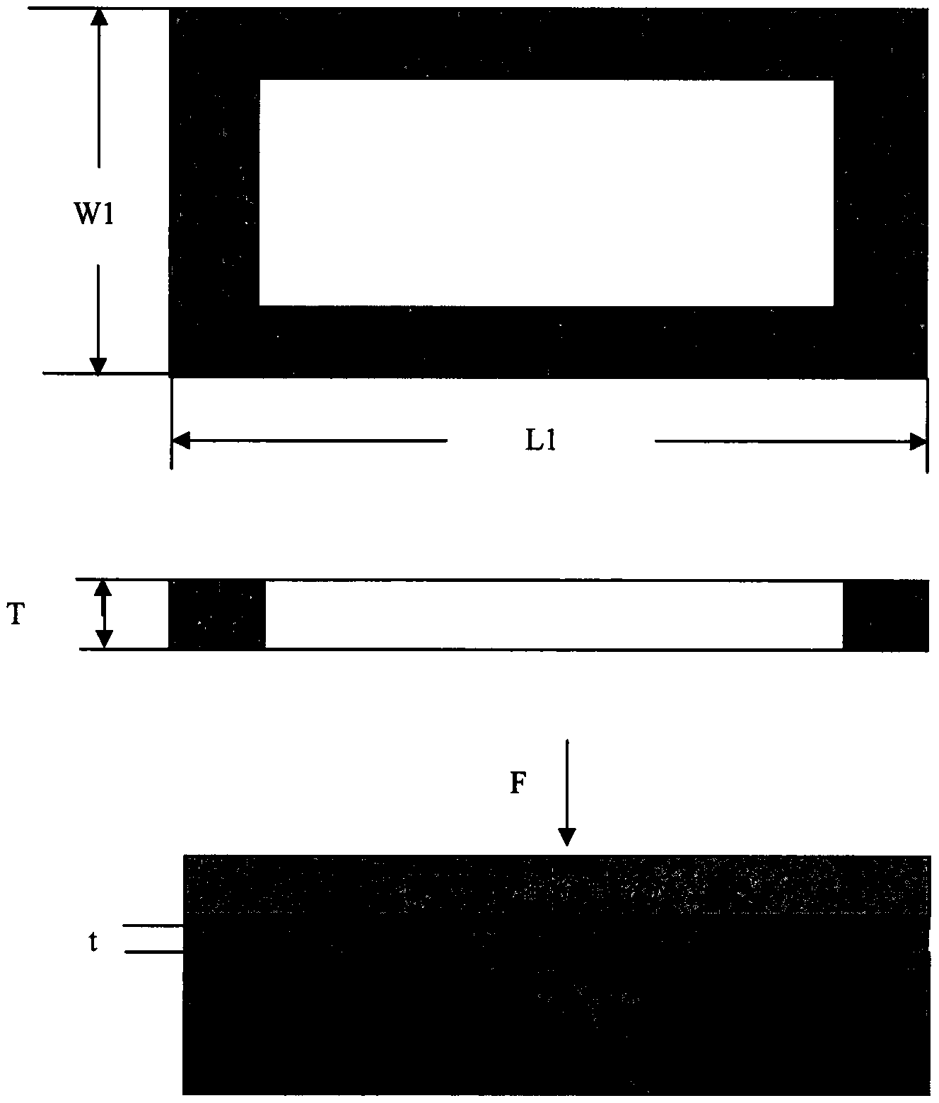
[0022] The present invention changes the existing solder from flux-containing solder paste to flux-free solder sheet by analyzing the relationship between the void rate of workpieces after soldering and the shape of solder. The void rate of the solder joint interface is composed of the air bubble rate + debonding rate, that is, the voids at the solder joint interface have debonding caused by non-wetting or inclusions in addition to air bubbles. Flux residue and oxidation are the main factors leading to debonding. The use of flux can effectively remove the oxide layer on the surface of the solder and the pad, improving soldering reliability, but at the same time, it is easy to produce flux residues, resulting in debonding; without using flux, the oxide layer cannot be removed, and the solder is difficult to wet on the pad surface, thus cause debonding. Therefore, we choose to use soldering sheet instead of soldering paste to eliminate the negative impact of flux. At the same t...


PUM


Abstract

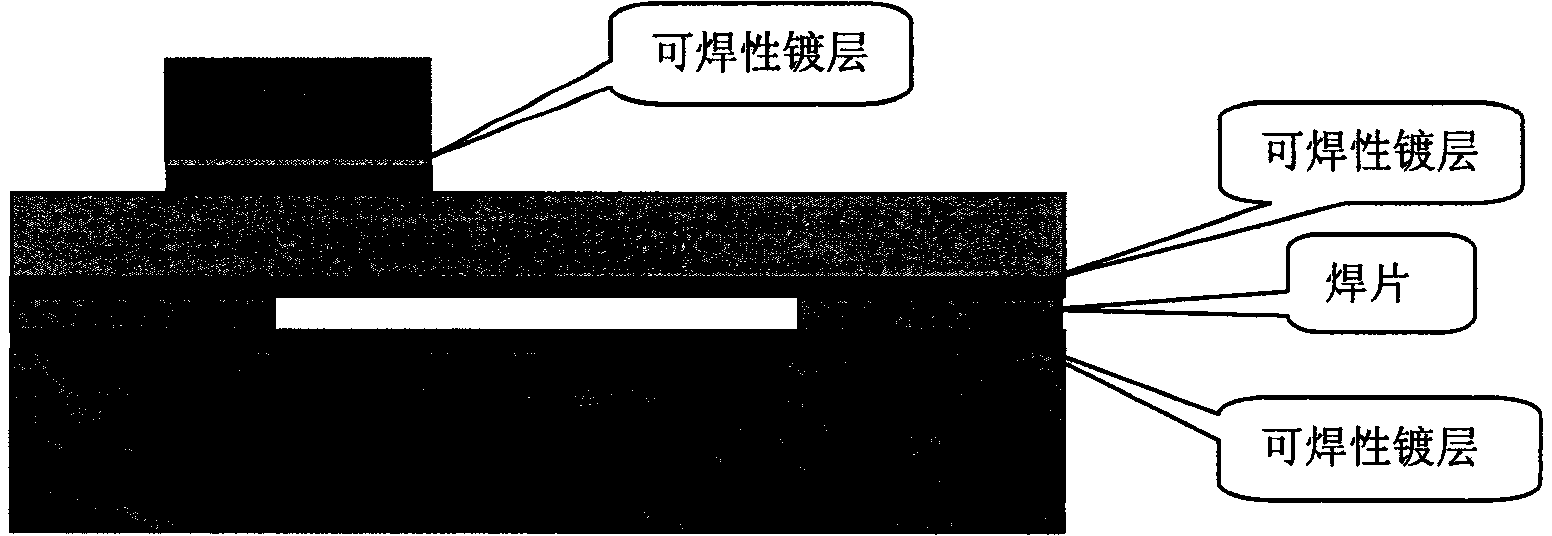
A high brazing rate vacuum welding method based on plasma cleaning, the steps are as follows: (1) plasma cleaning the solder sheet; The shape of the parts is the same, and the middle is hollowed out to form a gasket shape; (3) The welded workpiece, the solder piece, and the carrier are superimposed together in sequence, and a certain weight of tooling is added to exert pressure on the welded workpiece; (4) The superimposed good The workpiece is placed on the heating platform at room temperature, and the heating platform is placed in the vacuum furnace cavity, and the vacuum is started until the vacuum degree is less than 100Pa. At this time, the temperature of the solder piece is at room temperature; (5) The heating platform preheats the workpiece, and keep warm; (6) continue heating until the melting point of the solder sheet is 30-40°C above, and keep warm; (7) backfill the vacuum furnace cavity with the atmosphere, so that the air pressure in the cavity where the workpiece is located returns to atmospheric pressure; (8) cool down until the solder Below the melting point of the sheet, the welding is completed.

Description

technical field [0001] The invention relates to a flux-free vacuum welding method with a high brazing rate of a ceramic circuit board and a heat sink carrier, which combines plasma cleaning, vacuum release and solder piece shape design to achieve a high brazing rate with a void rate of less than 3%. Background technique [0002] Some power chips need to be installed in power electronic products such as secondary power supply, drive circuit and other modules, and the thermal conductivity of printed circuit boards is low, which cannot meet the heat dissipation requirements of power circuits. Therefore, power chips need to be installed on ceramic circuit boards and heat sinks. On components welded by heat sink carriers with high conductivity. The void rate of the soldering interface between the ceramic board and the heat sink carrier has always been a hot spot of concern, because for power devices with high heat dissipation requirements, the reliability of the device directly d...

Claims


Application Information

Patent Timeline
Patent Type & Authority Patents(China)
IPC IPC(8): B23K35/14B23K1/008
Inventor 杨猛陈雅容胡凤达高伟娜
Owner BEIJING SATELLITE MFG FACTORY
Learn More