Method for efficiently grinding and polishing GaN chips

A high-efficiency, wafer-based technology, applied in the direction of grinding equipment, grinding machine tools, electrical components, etc., can solve the problems of difficult to obtain high-quality polished surface, accelerate GaN surface oxidation corrosion, long polishing cycle and low efficiency, and achieve improved flatness and roughness, prevent mechanical scratches, improve the effect of flatness

Inactive Publication Date: 2016-11-23
SINO NITRIDE SEMICON
View PDF9 Cites 20 Cited by
  • Summary
  • Abstract
  • Description
  • Claims
  • Application Information

AI Technical Summary

Problems solved by technology

The polishing method of GaN wafers mainly adopts chemical mechanical polishing (CMP), which mainly uses chemical raw materials (polishing liquid) to chemically modify the surface to be polished, and then uses mechanical methods to remove the modified layer. This mechanically assisted polishing method is easy to cause surface damage. Mechanical damage, especially for GaN, a material with high hardness and high brittleness, often leaves surface scratches, making it difficult to obtain a high-quality polished surface
Chinese patents CN101220244A and CN 104364331 A improve the surface quality of polished GaN wafers by improving the compos

Method used


Image

  • Method for efficiently grinding and polishing GaN chips
  • Method for efficiently grinding and polishing GaN chips

Examples


Embodiment 1

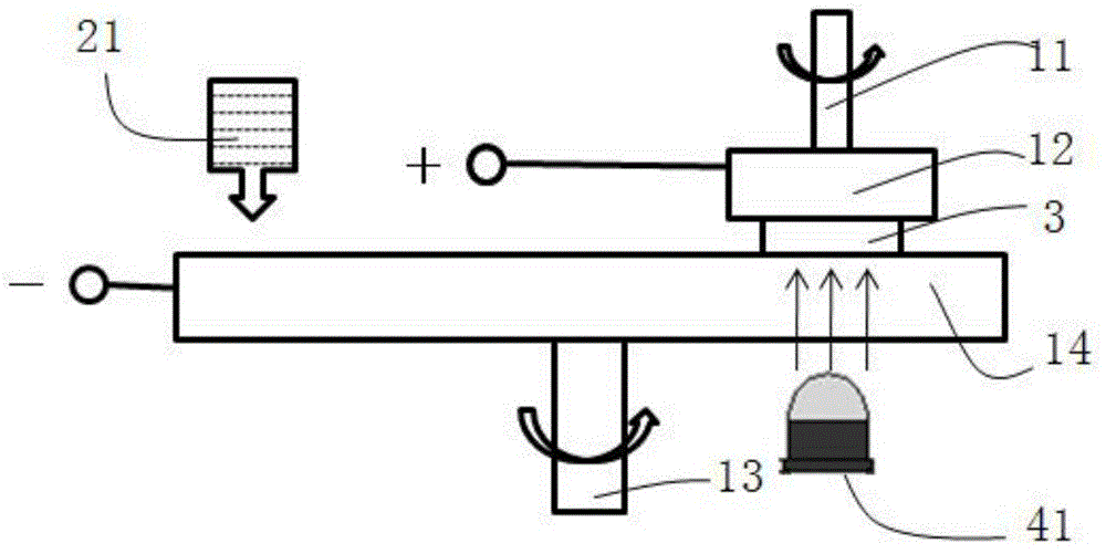
[0016] Such as figure 1 As shown, the upper tray 12 is connected to the positive pole of the power supply, and its rotation is realized through the upper rotating shaft 11 , and the lower polishing disc 14 is connected to the negative pole of the power supply, and its rotation is realized through the lower rotating shaft 13 . The cleaned and dried GaN wafer 3 is fixed on the upper tray 12 of the polishing device, so that the surface to be polished of the GaN wafer 3 faces the front of the lower polishing disc 14 and is in a contact or semi-contact state; the light source 41 is turned on to illuminate the GaN wafer 3 on the surface to be polished; set the appropriate voltage value and turn on the power to make the upper tray 12, the GaN wafer 3 to be polished, and the lower polishing disc 14 form a current loop; after a certain oxide layer is formed on the surface to be polished, the polishing liquid 21 is sprayed to open the polishing device. All rotation procedures, and apply...

Embodiment 2

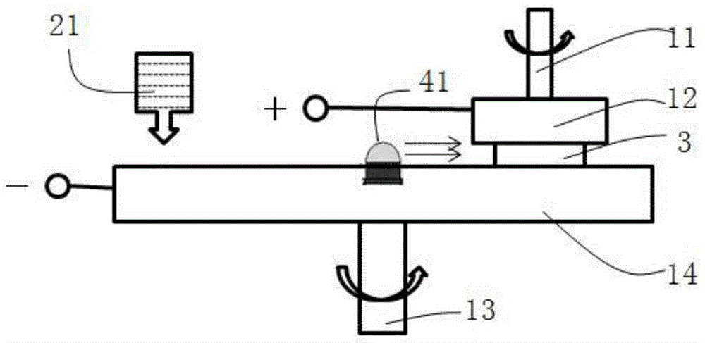
[0018] Such as figure 2 As shown, the upper tray 12 is connected to the positive pole of the power supply, and its rotation is realized through the upper rotating shaft 11 , and the lower polishing disc 14 is connected to the negative pole of the power supply, and its rotation is realized through the lower rotating shaft 13 . The cleaned and dried GaN wafer 3 is fixed on the upper tray 12 of the polishing device, so that the surface to be polished of the GaN wafer 3 faces the front of the lower polishing disc 14 and is in a semi-contact state; Side and the surface to be polished; set the appropriate voltage value and turn on the power to make the upper tray 12, the GaN wafer 3 to be polished, and the lower polishing disc 14 form a current loop; after a certain oxide layer is formed on the surface to be polished, spray the polishing liquid 21, and open the polishing device. All rotation procedures, and apply suitable downward pressure on the upper tray 12, remove the oxide lay...


PUM


Abstract

The invention provides a method for efficiently grinding and polishing GaN chips, namely the photoelectrochemistry mechanical polishing method for efficiently grinding the GaN chips. The method includes the steps that under the effects of illumination and an external electric field, the to-be-polished surfaces of the GaN chips are oxidized to form gallium oxide, the gallium oxide and hydroxyl ions in a polishing solution are combined to form gallium hydroxide passivation layers, and the gallium oxide and hydrogen ions in the polishing solution are combined to form gallium ions; and under the protection of the gallium hydroxide passivation layers and the polishing solution rich in gallium ion, illumination and oxidation on concave parts of the to-be-polished surfaces are effectively restrained, high convex parts of the to-be-polished surfaces are mechanically removed, and new GaN surfaces are exposed and continue to be selectively removed through illumination and oxidation. The illumination intensity, voltage values and pressure applied to an upper tray are regulated and controlled, the oxidation speed of the to-be-polished surfaces of the chips is matched with the mechanical removing speed, and therefore the surface flatness and polishing efficiency of the GaN chips are improved, and high-quality polished GaN chips are obtained.

Description

technical field [0001] The invention relates to the technical field of semiconductor optoelectronic materials, in particular to a photoelectrochemical mechanical method for grinding and polishing GaN wafers with high efficiency. Background technique [0002] Gallium Nitride (GaN) has been extensively researched and applied due to its excellent performance, which can be applied to the preparation of high-power high-frequency devices and other semiconductor devices that work under special conditions. The crystal quality of the GaN epitaxial layer is the fundamental guarantee for the realization of high-performance GaN-based devices. The use of GaN single crystal substrates to realize homoepitaxy is the main way to improve the crystal quality of GaN epitaxial layers and GaN-based devices. [0003] GaN single crystal substrates generally undergo surface treatment such as grinding and polishing before epitaxy, so as to obtain crystal planes that are conducive to crystal epitaxia...

Claims


Application Information

Patent Timeline
IPC IPC(8): B24B37/10H01L21/306H01L33/00
CPCB24B37/10H01L21/30625H01L33/0075
Inventor 刘南柳陈蛟张国义
Owner SINO NITRIDE SEMICON
Why Eureka
Try Eureka